Stack type chip packaging structure, chip packaging structure and manufacture process

A chip packaging structure, packaging structure technology, applied in semiconductor/solid-state device manufacturing, electrical components, electrical solid-state devices, etc., to achieve the effect of improving integration and saving available space

Active Publication Date: 2008-02-06
ADVANCED SEMICON ENG INC
View PDF0 Cites 5 Cited by
  • Summary
  • Abstract
  • Description
  • Claims
  • Application Information

AI Technical Summary

Problems solved by technology

[0008] Another object of the present invention is to provide a chip packaging structure, which can be applied to the above-mentioned stacked chip packaging structure, so as to solve the problems of the existing chip packaging structure technology

Method used


Image

  • Stack type chip packaging structure, chip packaging structure and manufacture process
  • Stack type chip packaging structure, chip packaging structure and manufacture process
  • Stack type chip packaging structure, chip packaging structure and manufacture process

Examples


Embodiment Construction

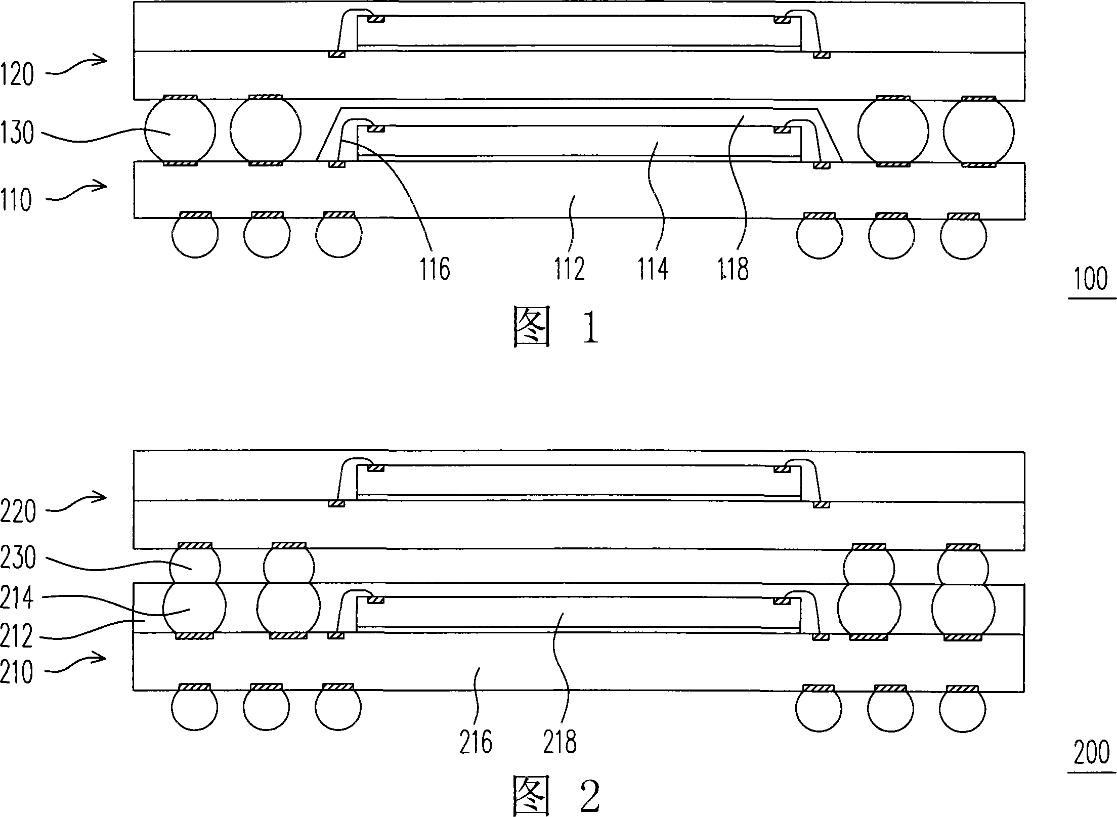
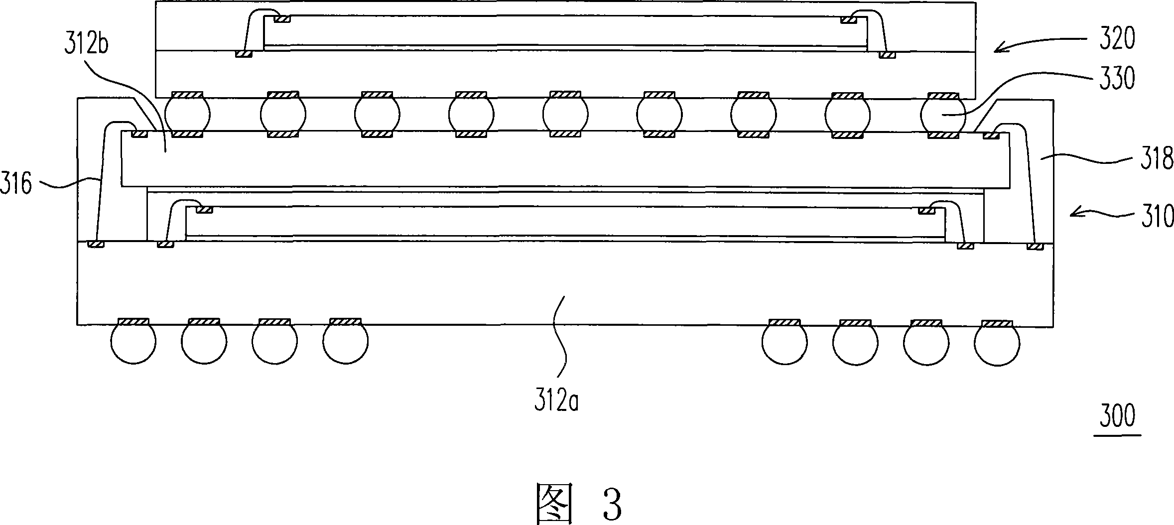
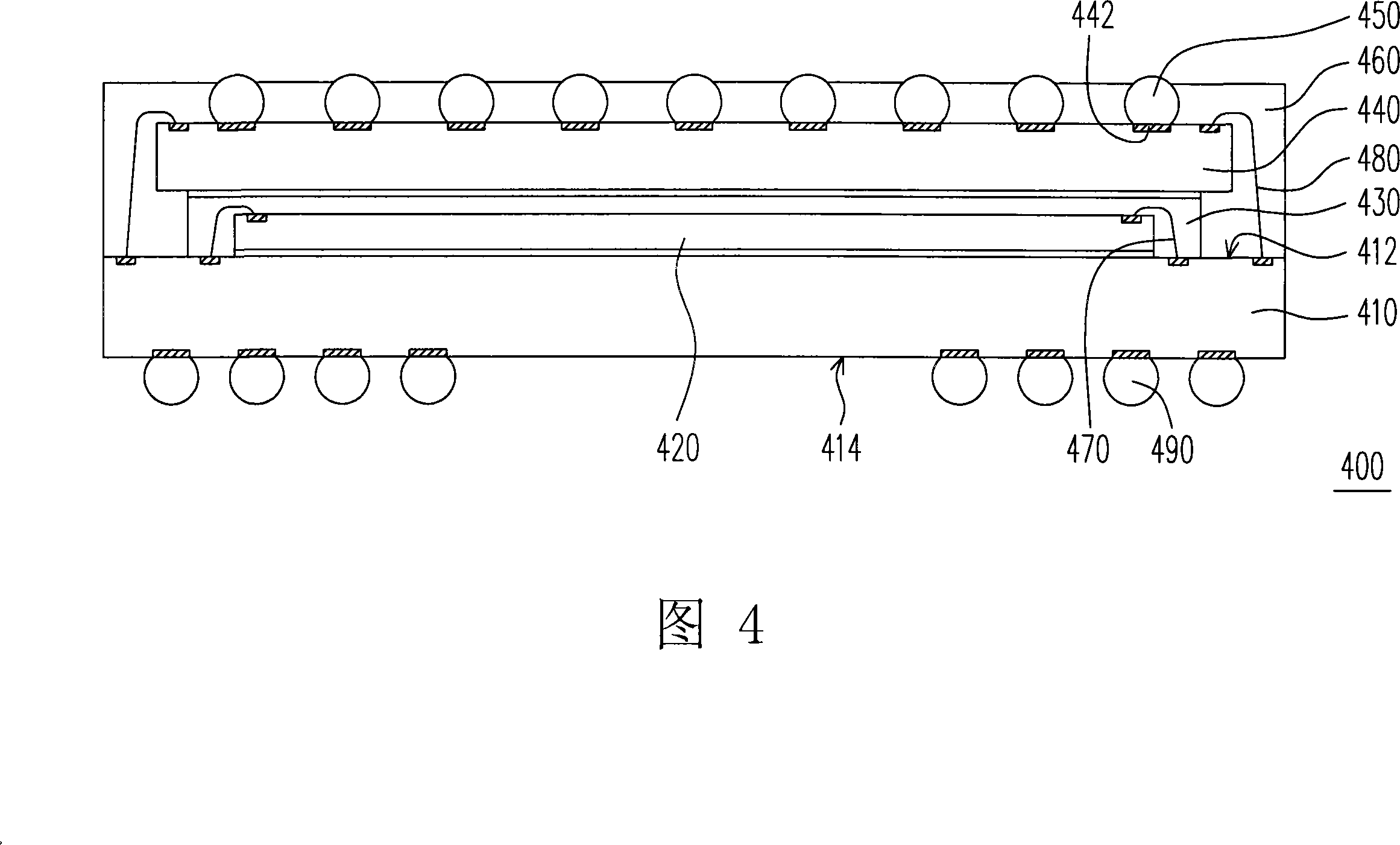
[0031] FIG. 4 is a schematic cross-sectional view of a chip packaging structure according to an embodiment of the present invention. Referring to FIG. 4 , the chip packaging structure 400 of this embodiment includes a carrier 410 , a chip 420 , a first encapsulant 430 , a wiring element 440 , a plurality of conductive elements 450 , and a second encapsulant 460 . The carrier 410 has a carrying surface 412 and an opposite back surface 414 . The chip 420 is disposed on the carrying surface 412 and electrically connected to the carrier 410 . The first encapsulant 430 is disposed on the carrying surface 412 and covers the chip 420 . The wiring element 440 is disposed on the first encapsulant 430 and electrically connected to the carrier 410 , and the wiring element 440 provides a plurality of pads 442 above the surface of the first encapsulant 430 . The conductive elements 450 are respectively disposed on the pads 442 . The second encapsulant 460 covers the carrying surface 412...


PUM


Abstract

The present invention discloses a stacked chip encapsulation structure, a chip encapsulation structure and the making process therein, which includes a first encapsulation structure unit and a second encapsulation structure unit. Wherein, the first encapsulation structure unit has a loader, a chip, a first sealant, a wire distribution element, a conductive element; and a second sealant covers the loader surface, the chip, the first sealant, the wire distribution element and the conductive element and are exposed out of the top of the conductive element; moreover, the second encapsulation structure unit realizes electric connection with the wire distribution element through the conductive element. By using a wire distribution element connecting two encapsulation structure units, the present inventionsaves the useable space of the loader and improves the integration degree; moreover, as the sealant covers the whole loading surface, the figure is not influenced by the size and configuration of the chip, therefore, the sealant mould of the making process of the invention can have various chip sizes and configurations.

Description

【Technical field】 [0001] The present invention relates to a semiconductor device package structure and its manufacturing process, and in particular to a stacked type chip packaging structure and its manufacturing process. 【Background technique】 [0002] In today's highly informationized society, the market for multimedia applications continues to expand rapidly, and integrated circuit (IC) packaging technology also needs to develop in line with the trend of digitization, networking, regional connection, and humanization of electronic devices. In order to achieve the above requirements, it is necessary to strengthen the requirements of high-speed processing, multi-function, integration, small size, light weight and low price of electronic components, so the integrated circuit packaging technology is also developing towards miniaturization and high density. . In addition to the existing common Ball Grid Array (BGA), Chip-Scale Package (CSP), and Flip Chip package (F / C package...

Claims


Application Information

Patent Timeline
Patent Type & Authority Applications(China)
IPC IPC(8): H01L25/00H01L25/065H01L23/488H01L23/31H01L21/50H01L21/60H01L21/56
CPCH01L2224/48091H01L2924/15311
Inventor 李玉麟翁国良
Owner ADVANCED SEMICON ENG INC
Why Eureka
Try Eureka