Chemical and mechanical grinding method

A grinding method and chemical-mechanical technology, used in surface polishing machine tools, grinding/polishing equipment, electrical components, etc., can solve the problems of corrosion and easy contamination of wafer surface materials, and achieve the effect of corrosion inhibition and good effect.

Inactive Publication Date: 2008-02-13
SEMICON MFG INT (SHANGHAI) CORP +1
View PDF1 Cites 6 Cited by
  • Summary
  • Abstract
  • Description
  • Claims
  • Application Information

AI Technical Summary

Problems solved by technology

[0003] The purpose of the present invention is to provide a chemical mechanical polishing method to solve the problem that in the existing chemical mechanical polishing method, when multiple wafers are simultaneously polished, the wafer surface material is easily polluted or corroded before entering the next step

Method used


Image

  • Chemical and mechanical grinding method
  • Chemical and mechanical grinding method
  • Chemical and mechanical grinding method

Examples


Embodiment Construction

[0022] In order to make the above objects, features and advantages of the present invention more comprehensible, specific implementations of the present invention will be described in detail below in conjunction with the accompanying drawings.

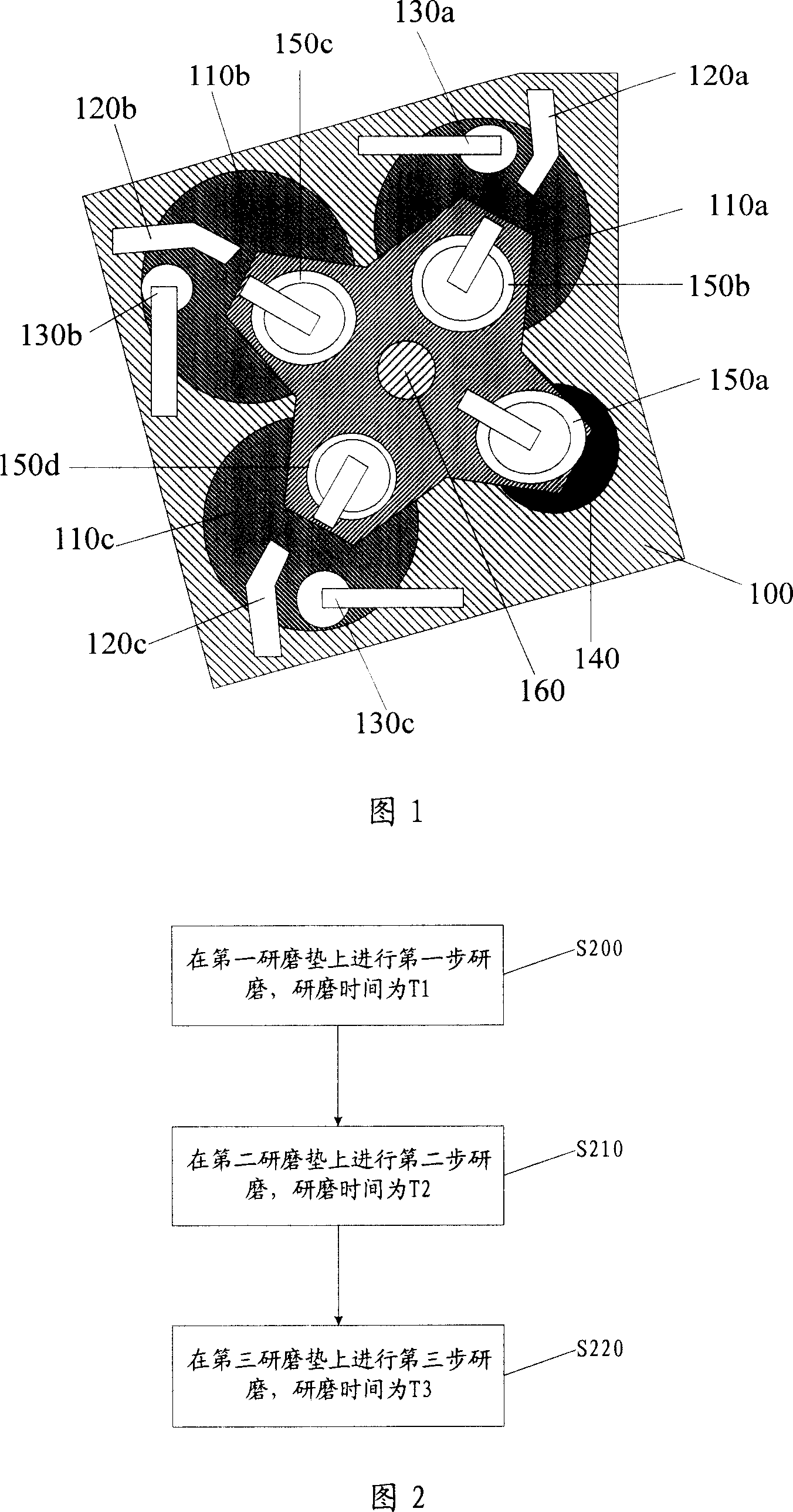
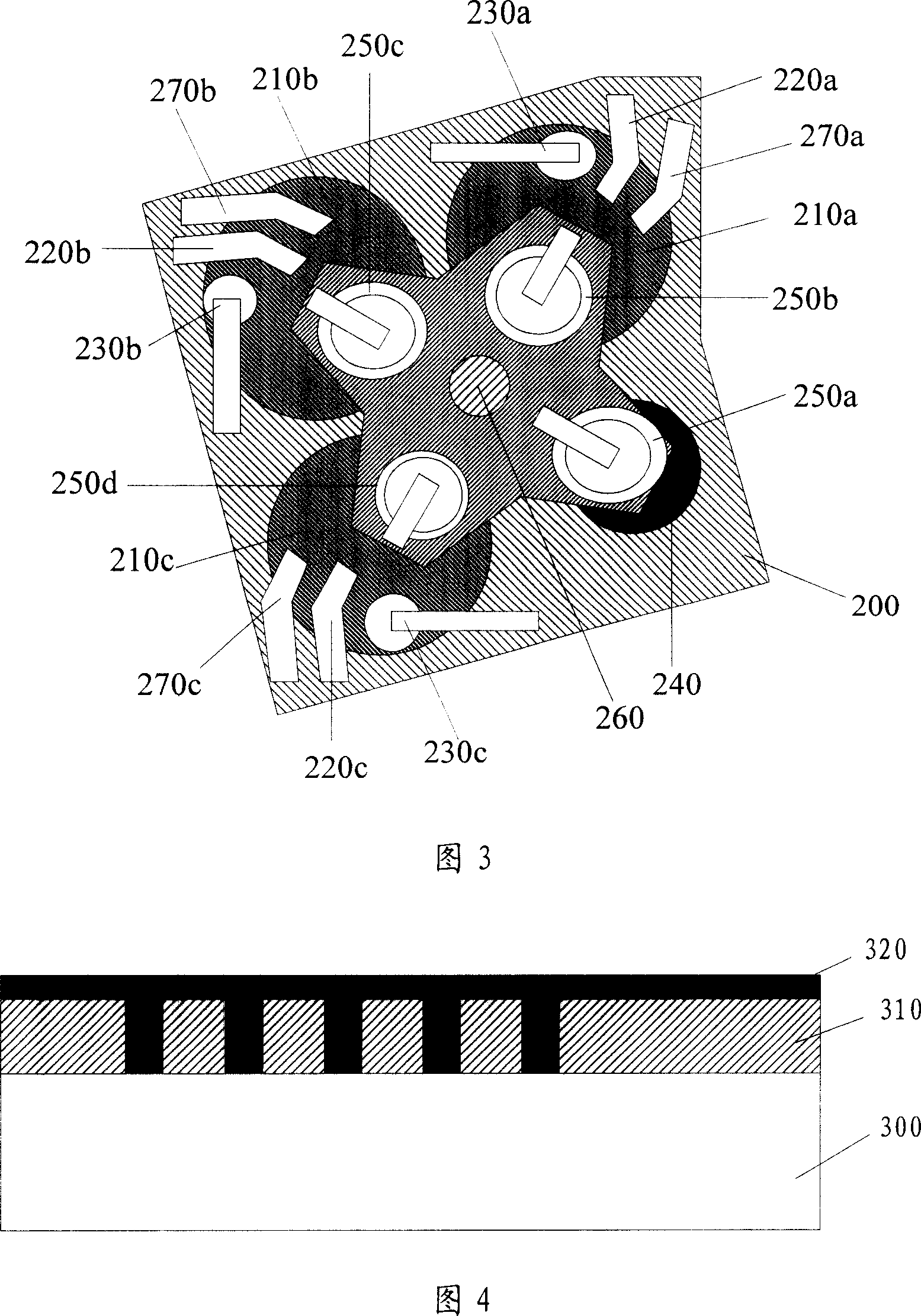
[0023] Chemical mechanical polishing is a planarization method that removes the material layer on the wafer surface through a combination of chemical and mechanical methods. Grinding is generally divided into several steps, for example, coarse grinding, fine grinding, and the like. Each step is done on a different polishing pad. A grinding device will have several grinding pads and several grinding heads, and the wafer will be sucked by the grinding head and the material layer to be ground on the wafer will be pressed down to the surface of the grinding pad, and there will be a grinding pad between the grinding pad and the wafer surface. Liquid (Slurry), through the relative rotation between the polishing pad and the grinding head, th...


PUM


Abstract

A chemical-mechanical grinding method comprises that a plurality of grinding pads and grinding heads are provided for material layers on the grinding chips; a plurality of antiseptic feed devices are provided and the antiseptic feed devices are used for supplying antiseptic to the grinding pads; the a plurality of grinding pads grind different chips at the same time; antiseptic is provided on the ground chip surface until all chips are ground. The method can prevent the chip surface from being polluted or corroded.

Description

technical field [0001] The invention relates to the technical field of semiconductor manufacturing, in particular to a chemical mechanical polishing method. Background technique [0002] With the increasing reduction of semiconductor devices, due to the excessive fluctuation of the wafer surface caused by the deposition process of multi-layer interconnection or filling aspect ratio, it is difficult to focus the lithography process, and the ability to control the line width is weakened, thereby reducing the overall wafer surface area. The consistency of the line width. The industry introduces chemical mechanical planarization (CMP), that is, the silicon wafer is placed on a grinding head, and the surface of the silicon wafer is brought into contact with a polishing pad, and the relative movement between the surface of the silicon wafer and the polishing pad makes Silicon wafer surface planarization. In the CMP process, a slurry (Slurry) is supplied between the surface of th...

Claims


Application Information

Patent Timeline
Patent Type & Authority Applications(China)
IPC IPC(8): B24B29/02H01L21/304B24B57/02
Inventor 檀广节李强
Owner SEMICON MFG INT (SHANGHAI) CORP
Why Eureka
Try Eureka