

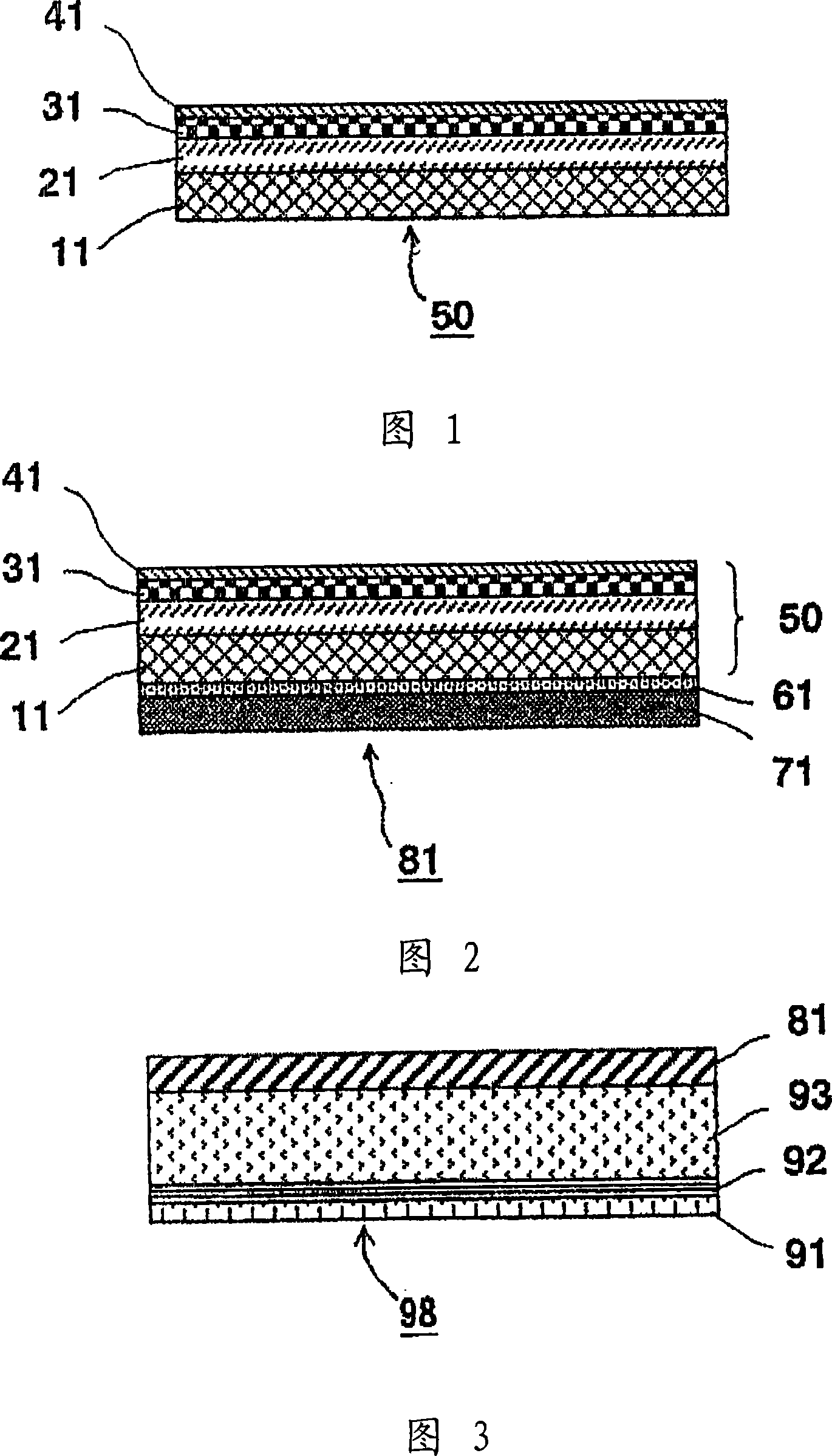
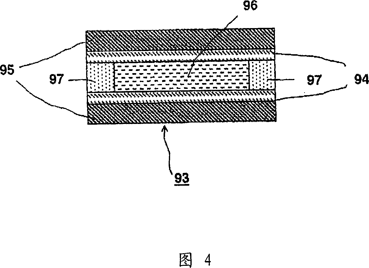
Optical laminated film for liquid crystal display device
A liquid crystal display device and optical layer technology, applied in optics, optical elements, nonlinear optics, etc., can solve the problems of poor contrast and poor visibility of light and dark display, and achieve excellent contrast, less glare and reflection, and light reflection. low rate effect
- Summary
- Abstract
- Description
- Claims
- Application Information
AI Technical Summary
Problems solved by technology
Method used
Image

Examples
Embodiment
[0261] The present invention will be described in detail through examples, but the present invention is not limited to the following examples. Wherein, unless otherwise specified, parts are based on weight.
[0262] Evaluation of physical properties in this example was performed by the following methods.
[0263] (1) Film thickness of base film (standard film thickness, film thickness fluctuation value)
[0264] The film is cut out corresponding to every 100 mm in the length direction, and the cut out film is measured corresponding to every It measures at 0.48 mm, and makes the arithmetic mean value of the measured value into reference film thickness T (micrometer). Regarding film thickness variation (film thickness variation), the maximum value among the above-mentioned measured film thicknesses is defined as T MAX (μm), the minimum value is set to T MIN (μm), and calculated according to the following formula.
[0265] Variation in film thickness (%) = (T MAX -T MIN ) / ...
manufacture example 1
[0286] Manufacturing example 1 Fabrication of Substrate Film 1A
[0287] Norbornene-based polymer (product name "ZEONOR 1420R", produced by ZEON Corporation of Japan; glass transition temperature 136°C, saturated water absorption less than 0.01% by weight) was carried out at 110°C using a hot air dryer that circulates air. 4 hours to dry. Then, the pellets were melt-extruded at 260° C. using a short shaft extruder having a coat hanger-shaped T-die with a die lip width of 650 mm to obtain a substrate film 1A with a width of 660 mm. A disc-shaped polymer filter (filtering precision of 30 μm) is used, and chrome plating with a surface roughness of Ra=0.05 μm is performed on the inner surface of the die lip. The obtained base film 1A has a volatile component content of 0.01% by weight or less, and a saturated water absorption rate of 0.01% by weight or less. In addition, the base film 1A had a base film thickness of 40 μm, a film thickness variation of 2.3%, and a die line dept...
manufacture example 2
[0288] Manufacturing example 2 Preparation of Composition H1 for Hard Coat Formation (n d 20 =1.62)
[0289] In the modified alcohol sol of 1000 parts by weight of antimony pentoxide (30% of solid content concentration, produced by Catalyst Chemical Industry Co., Ltd.), 100 parts by weight of ultraviolet curable urethane acrylate (produced by Japan Synthetic Chemical Co., Ltd., trade name is "Ultraviolet UV7000B") is mixed. , 4 parts by weight of a photopolymerization initiator (manufactured by Ciba-Geigy, trade name "Irugakiyua-184") to obtain composition H1 for forming an ultraviolet curable hard coat layer.
PUM
| Property | Measurement | Unit |
|---|---|---|
| depth | aaaaa | aaaaa |
| diameter | aaaaa | aaaaa |
| particle size | aaaaa | aaaaa |
Abstract
Description
Claims
Application Information