Semiconductor chip packaging process and its structure

A chip packaging structure and chip packaging technology, applied in semiconductor/solid-state device manufacturing, semiconductor devices, semiconductor/solid-state device components, etc., can solve problems such as limited application fields and hollow openings of semiconductor chips

Active Publication Date: 2008-02-27
ADVANCED SEMICON ENG INC
View PDF2 Cites 6 Cited by
  • Summary
  • Abstract
  • Description
  • Claims
  • Application Information

AI Technical Summary

Problems solved by technology

However, this process and structure cannot form hollow openings on the surface of the semiconductor chip, so it is not suitable for packaging image sensing elements or temperature and humidity sensing elements and other semiconductor chips that must be active in contact with the air. Therefore, its application limited field

Method used


Image

  • Semiconductor chip packaging process and its structure
  • Semiconductor chip packaging process and its structure
  • Semiconductor chip packaging process and its structure

Examples


Embodiment Construction

[0033]In order to further explain the technical means and effects that the present invention adopts to achieve the intended purpose of the invention, below in conjunction with the accompanying drawings and preferred embodiments, the semiconductor chip packaging process and its structure according to the present invention will be described according to its specific implementation, steps, and structure. , features and their effects are described in detail below.

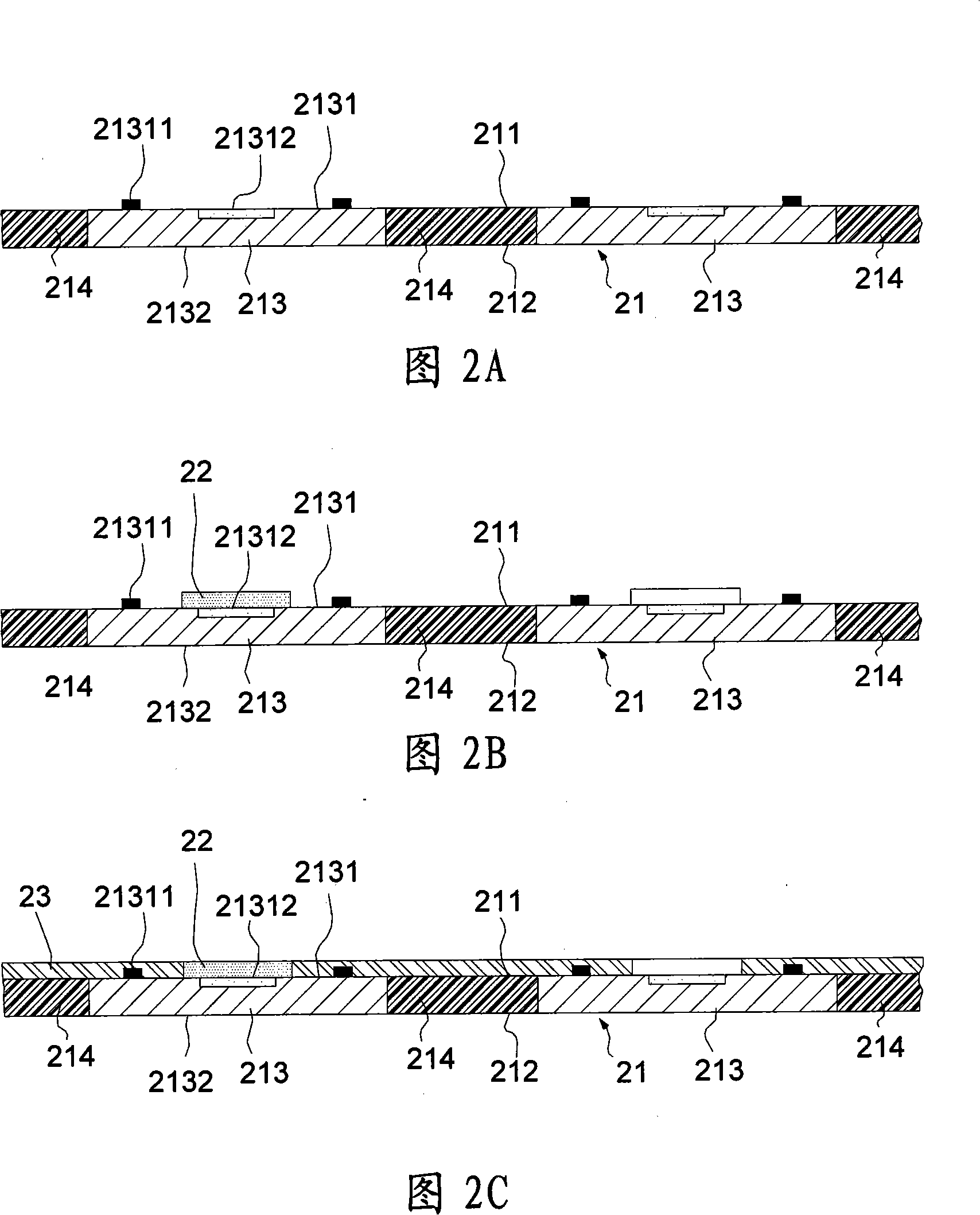
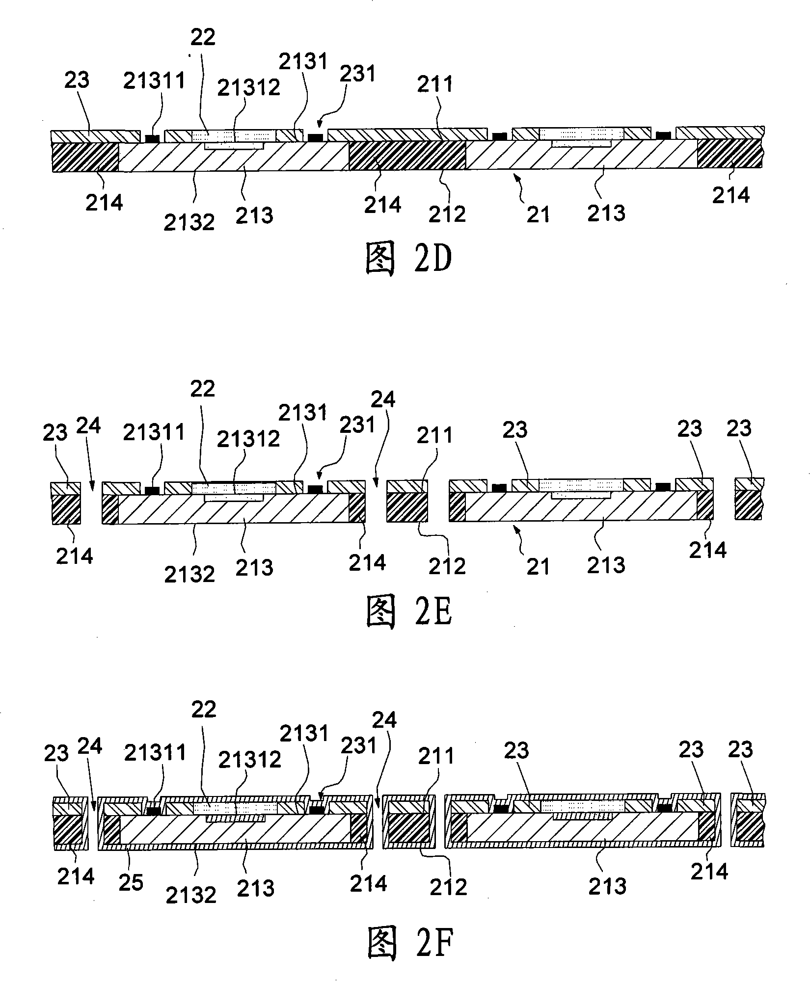
[0034] Please refer to FIG. 2A , FIG. 2B , FIG. 2C , FIG. 2D , FIG. 2E , FIG. 2F , FIG. 2G and FIG. 2H , which are schematic cross-sectional views of the manufacturing process of the first embodiment of the present invention. The manufacturing steps include: providing a substrate 21 in advance, the substrate 21 has an upper surface 211 and a lower surface 212, and the substrate 21 includes a plurality of image sensing chips 213 and an insulating colloid 214 surrounding the image sensing chips 213, Each image sensing ch...


PUM


Abstract

This invention is about a packaging manufacturing process of semiconductor chip and its structure, and its manufacturing process includes: provide a substrate containing an image sensor chip and insulation colloid, and its image sensor chips contains solder pad and active region; cover a transparent insulator on the active region; form an insulating layer on the surface of the substrate; open a number of openings to expose welding pad; form a number of cross-cutting holes on the outer surface of the image sensor chips, and these holes run through insulation layer and insulation colloid; form a metal layer on the surface of the insulation layer, opening, solder pad surface, pass through holes and the basement, and extend the solder pad to the bottom surface of the basement; pattern the bare metal layers to expose the top region of transparent insulation layer and remove part of the metal layer on the bottom surface of the substrate; cut and form packaging structure containing a single image sensor chip.

Description

technical field [0001] The invention relates to a semiconductor chip packaging process and its structure, in particular to a manufacturing method and structure of a non-bump packaging structure suitable for image sensing elements. Background technique [0002] Please refer to US Patent Publication No. 6,040,235 shown in FIG. 1A , which discloses a semiconductor chip packaging method. The patented technology is to cover an insulating material 120 on the active surface of a wafer 110, such as glass, which extends from the contact on the active surface of the wafer. to the backside of the wafer. After the wafer is cut into a plurality of chips, the contacts of each chip are extended to the surface of the package through the metal lines 130 . However, if there are too many chip defective products in each wafer, for example, half of the chips in a wafer are defective products, it is obviously not beneficial to use this packaging method. [0003] In addition, please refer to the...

Claims


Application Information

Patent Timeline
Patent Type & Authority Applications(China)
IPC IPC(8): H01L21/50H01L21/60H01L21/78H01L27/146H01L23/485
CPCH01L24/96H01L24/97H01L2224/04105H01L2224/19H01L2224/73267H01L2224/9222H01L2924/18162
Inventor 林千琪张志煌林悦农
Owner ADVANCED SEMICON ENG INC
Why Eureka
Try Eureka