Two-level SiC MOSFET H bridge main circuit topology with low parasitic oscillation

A low parasitic, main circuit technology, applied in the field of converters, can solve the problems that are not conducive to the application of SiC MOSFETs, increase the difficulty and time of circuit development, and achieve the effects of low cost, reduced loss, and reduced switching loss.

Inactive Publication Date: 2020-06-19
NANTONG UNIVERSITY
View PDF12 Cites 1 Cited by
  • Summary
  • Abstract
  • Description
  • Claims
  • Application Information

AI Technical Summary

Problems solved by technology

This increases the difficulty and time of circuit development, which is not conducive to the application of SiC MOSFETs in circuits

Method used


Image

  • Two-level SiC MOSFET H bridge main circuit topology with low parasitic oscillation
  • Two-level SiC MOSFET H bridge main circuit topology with low parasitic oscillation
  • Two-level SiC MOSFET H bridge main circuit topology with low parasitic oscillation

Examples


Embodiment Construction

[0027] The following will clearly and completely describe the technical solutions in the embodiments of the present invention with reference to the accompanying drawings in the embodiments of the present invention. Obviously, the described embodiments are only some, not all, embodiments of the present invention. Based on the embodiments of the present invention, all other embodiments obtained by persons of ordinary skill in the art without making creative efforts belong to the protection scope of the present invention.

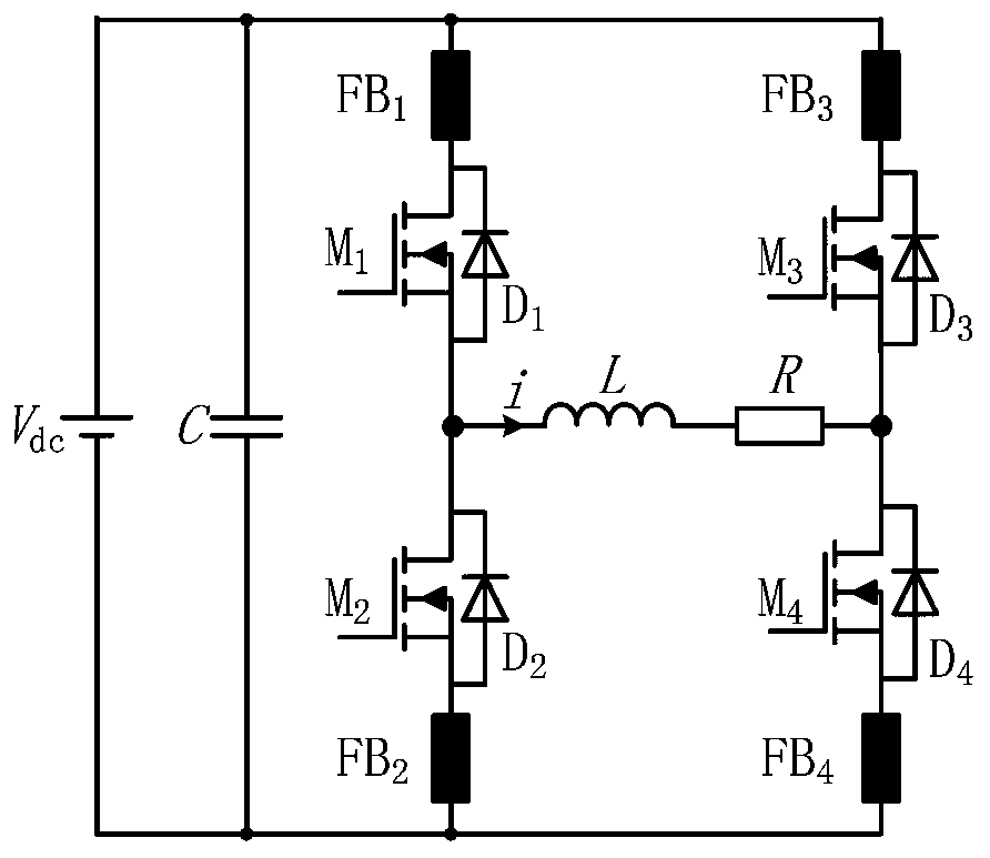
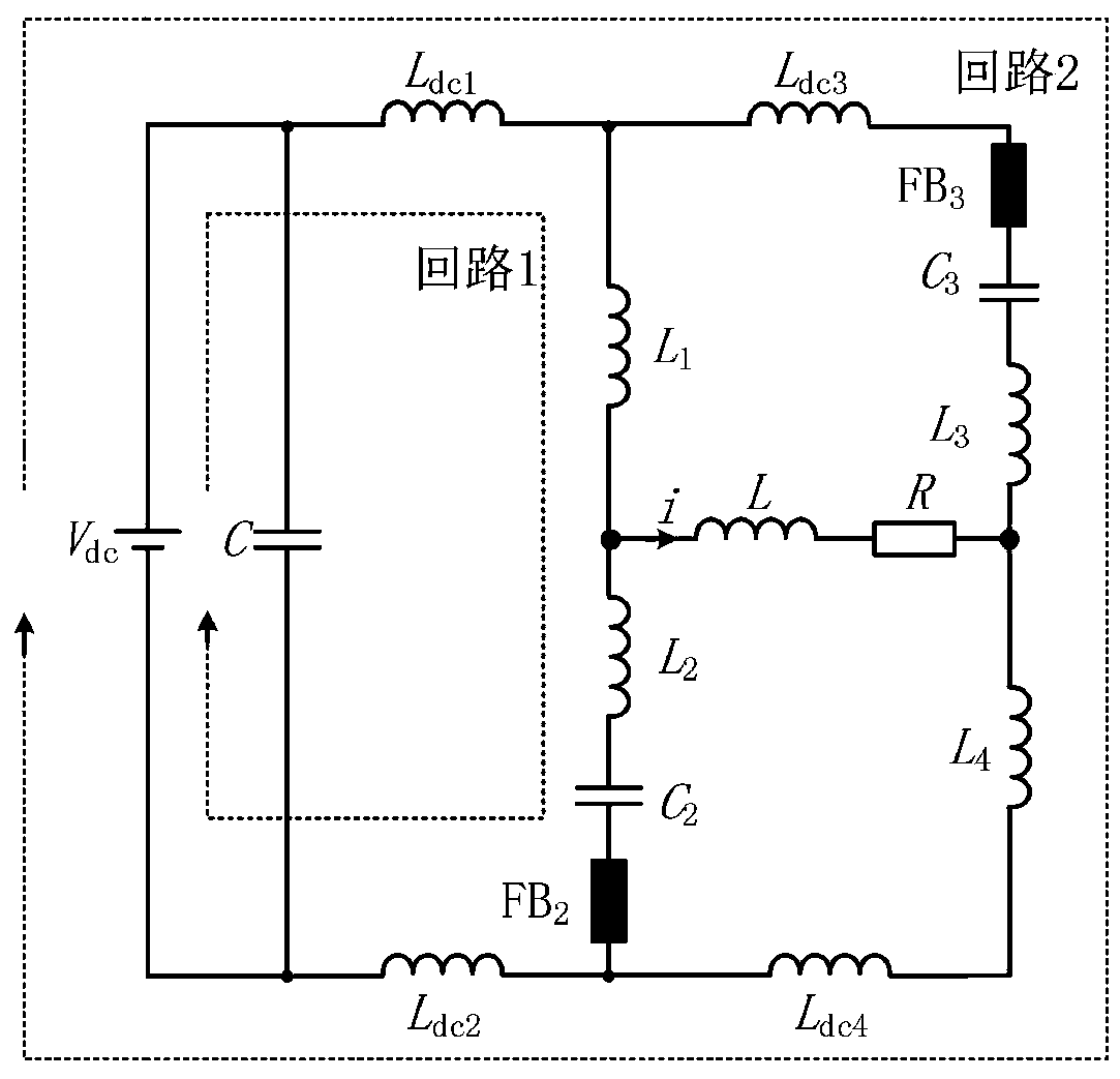
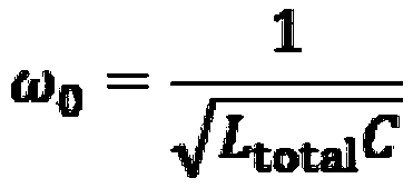
[0028] see Figure 1-2 , the present invention provides a technical solution: a low parasitic oscillation two-level SiC MOSFET H-bridge main circuit topology, characterized in that: the topology is composed of the following components: DC power supply V dc , DC bus capacitor C, load inductance L, load resistance R, 4 ferrite beads, respectively the first ferrite bead FB 1 , the second ferrite bead FB 2 , the third ferrite bead FB 3 , the fourth ferrite bead...


PUM


Abstract

The invention discloses a two-level SiC MOSFET H bridge main circuit topology with low parasitic oscillation. The topology is composed of the following components: a direct current power supply Vdc, adirect current bus capacitor C, a load inductor L, a load resistor R, four ferrite magnetic beads FB1, FB2, FB3 and FB4, four SiC MOSFETs M1, M2, M3 and M4, and four antiparallel diodes D1, D2, D3 and D4. The ferrite magnetic bead FB1, the SiC MOSFET M1, the SiC MOSFET M2 and the ferrite magnetic bead FB2 are sequentially connected in series to form a first half bridge; the ferrite magnetic beadFB3, the SiC MOSFET M3, the SiC MOSFET M4 and the ferrite magnetic bead FB4 are sequentially connected in series to form a second half bridge; the load inductor L and the load resistor R are connectedbetween the SiC MOSFET M1 and the SiC MOSFET M2 and are connected with the middle of the SiC MOSFET M3 and the middle of the SiC MOSFET M4; and the direct current power supply Vdc is connected with the direct current bus capacitor C and two half bridges in parallel. In the topology, the key components of the magnetic beads FB1, FB2, FB3 and FB4 play a role in suppressing parasitic oscillation ofthe circuit.

Description

technical field [0001] The invention relates to the technical field of converters, in particular to a low parasitic oscillation two-level SiC MOSFET H-bridge main circuit topology. Background technique [0002] At present, the two-level H-bridge circuit is widely used in photovoltaic power generation, micro-inverter power supply and other occasions. The traditional two-level H-bridge circuit uses Si IGBT (Insulated Gate Bipolar Transistor, insulated gate bipolar transistor) as the switching device. However, due to the insufficient performance of Si IGBT, it is difficult to further develop the two-level H-bridge circuit. Compared with Si IGBT, SiC MOSFET (Metal-Oxide-Semiconductor Field-Effect Transistor, Metal-Oxide-Semiconductor Field-Effect Transistor), as one of the new wide bandgap power electronic devices, has high operating junction temperature, high voltage level, switch High frequency, fast switching speed, low switching loss and other advantages. These advantages...

Claims


Application Information

Patent Timeline
Patent Type & Authority Applications(China)
IPC IPC(8): H02M7/483
CPCH02M7/483H02M1/0038H02M1/0054Y02B70/10
Inventor 张雷李雅任磊杨德健赵靖琳季润阳
Owner NANTONG UNIVERSITY
Why Eureka
Try Eureka