Piezoelectric ceramic driving circuit used for optical fiber stress adjustment

A piezoelectric ceramic drive, optical fiber stress technology, applied in the direction of piezoelectric effect/electrostrictive or magnetostrictive motors, generators/motors, electrical components, etc., can solve the problem of slow input voltage changes and achieve good dynamic Response characteristics, the effect of good follow-up zoom function

Inactive Publication Date: 2008-02-27
JILIN UNIV
View PDF0 Cites 49 Cited by
  • Summary
  • Abstract
  • Description
  • Claims
  • Application Information

AI Technical Summary

Problems solved by technology

Although this kind of circuit can finally output a relatively stable amplified voltage, there is often a long transition process bef

Method used


Image

  • Piezoelectric ceramic driving circuit used for optical fiber stress adjustment
  • Piezoelectric ceramic driving circuit used for optical fiber stress adjustment
  • Piezoelectric ceramic driving circuit used for optical fiber stress adjustment

Examples


Embodiment 1

[0040] Embodiment 1 Circuit structure and working principle of the present invention

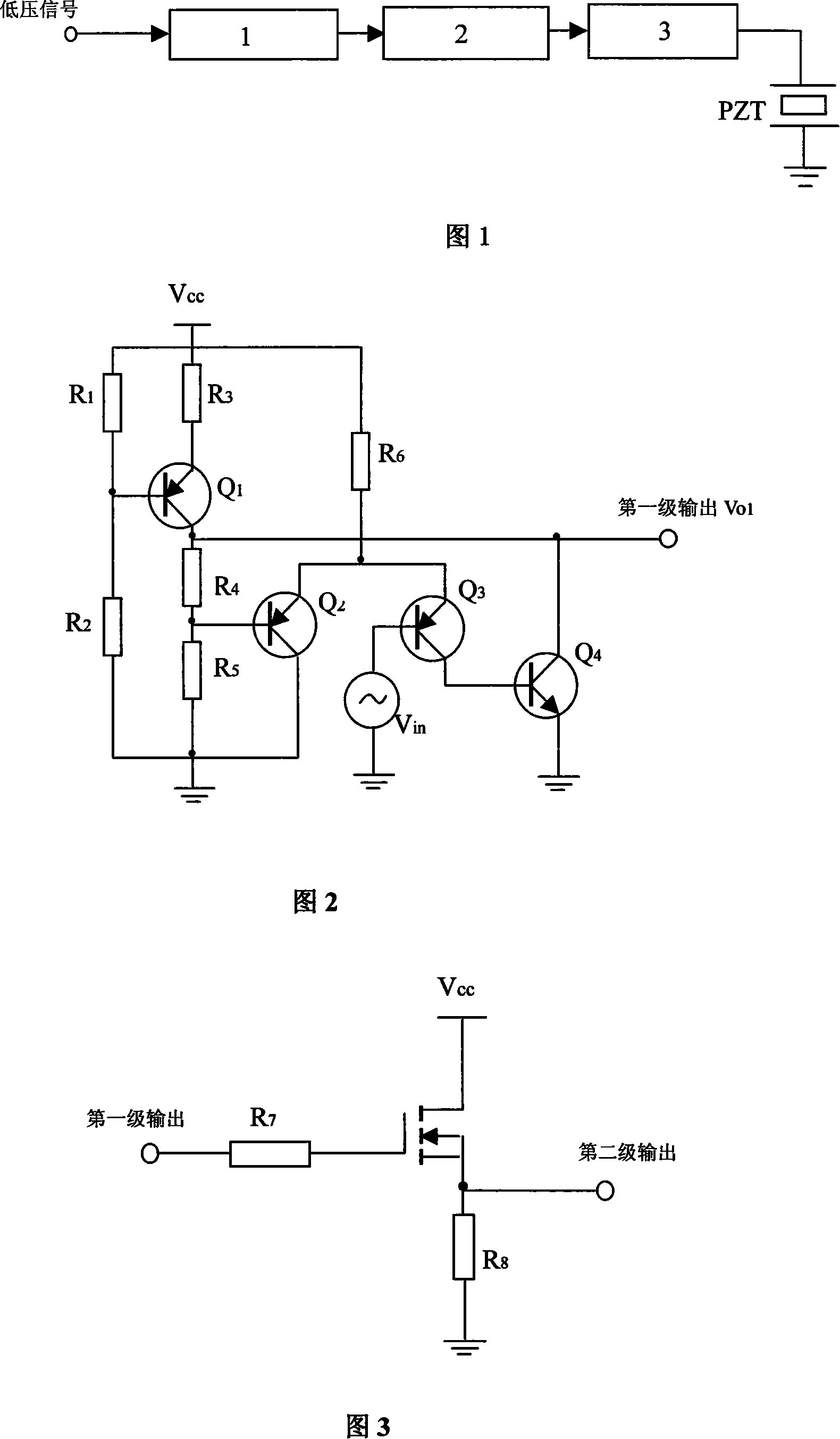
[0041] As shown in Figure 1: the piezoelectric ceramic (PZT) drive circuit applied to optical fiber stress regulation includes a voltage amplifier circuit (1), a power amplifier circuit (2) and a discharge loop circuit (3).

[0042] The voltage amplification stage circuit (1) is shown in Figure 2: Q 1 and resistor R 1 , R 2 , R 3 Consists of a constant current source circuit, where the transistor Q 1 base and resistor R 1 , R 2 connected, the emitter through a resistor R 3 with power supply V cc connection, R 2 Connect to ground, R 1 the other end with V cc connect. Resistance R 4 , R 5 , R 6 with transistor Q 2 , Q 3 Form a feedback comparison loop, where the transistor Q 2 , Q 3 For two PNP transistors with the same parameters, Q 2 , Q 3 The emitter is connected through resistor R 6 with power supply V cc connect, Q 2 Base connection resistance R 4 , R 5 , resistor...

Embodiment 2

[0049] Embodiment 2 A group of specific circuit parameters

[0050] A group of specific circuit parameters are provided below, but the circuit parameters of the present invention are not limited to this group:

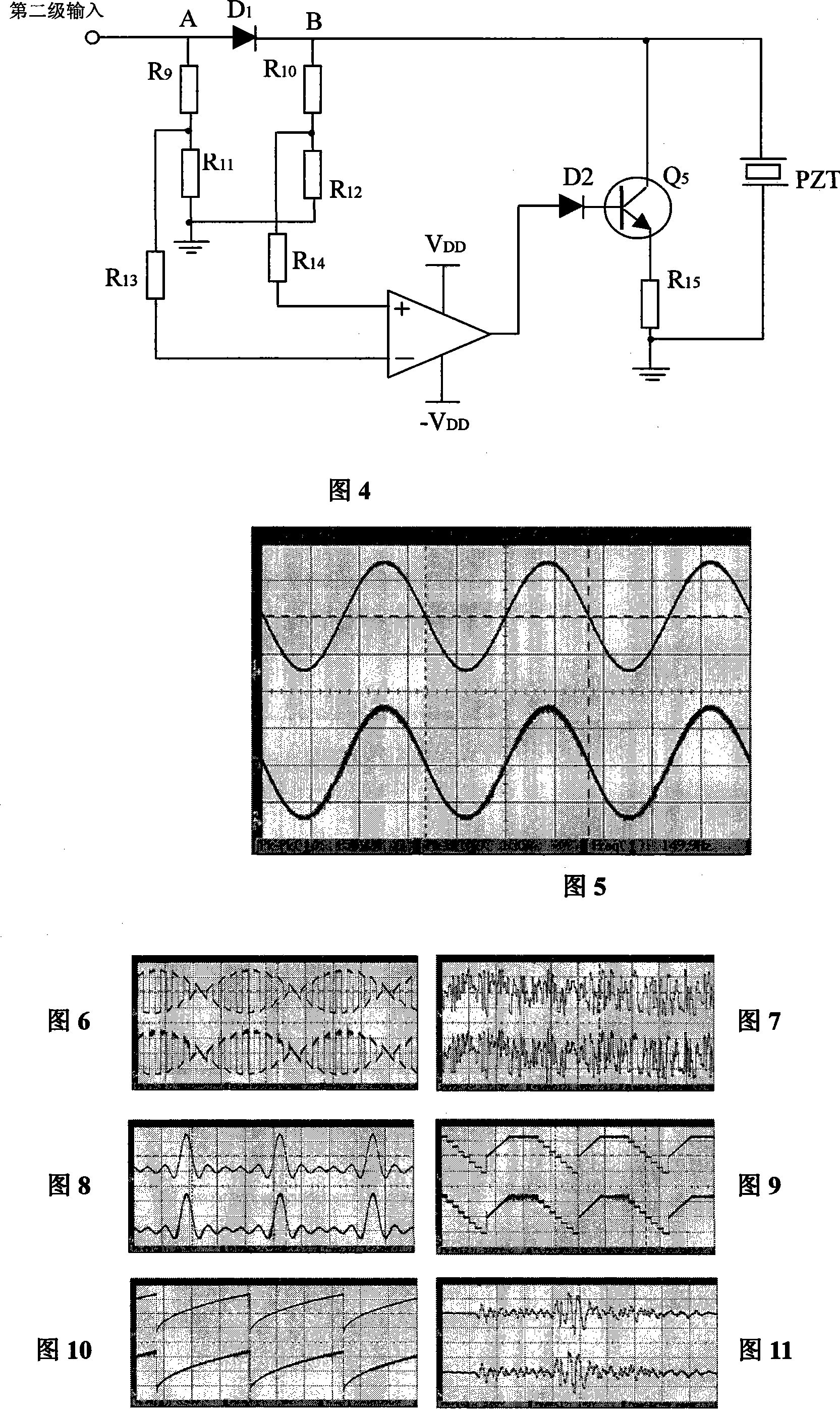
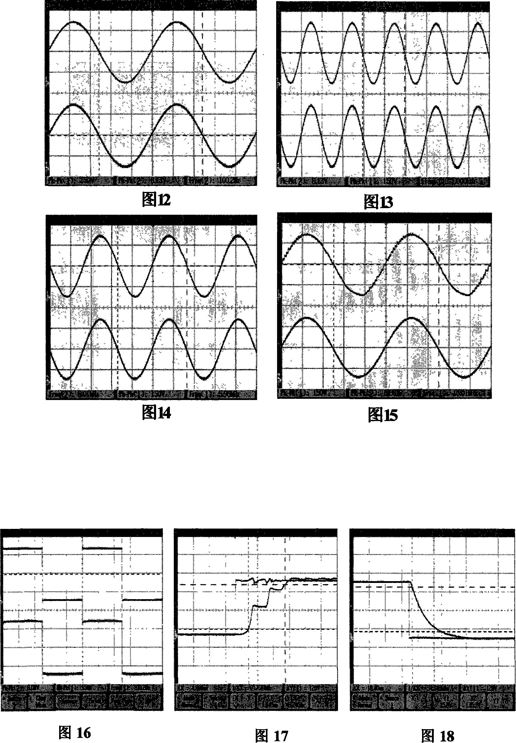
[0051] The preferred circuit parameters of the present invention are set as follows: V CC =230V, comparator operational amplifier voltage V DD = 5V, R 1 =300KΩ, R 2 = 400KΩ, R 3 =6.51KΩ, R 4 = 30KΩ, R 5 = 1.2KΩ, R 6 =150KΩ, R 7 = 1.0KΩ, R 8 = 20KΩ, R 9 =R 10 = 1.0MΩ, R 11 =R 12 =R 13 =R 14 = 10KΩ, R 15 = 10Ω.

Embodiment 3

[0052] Embodiment 3 The example of the driving circuit voltage magnification research of the present invention

[0053] The voltage magnification of the drive circuit of the present invention is studied using the circuit parameters set in Example 2. The amplified waveform of the sinusoidal input voltage shown in Figure 5 is obtained, where the upper part of the figure is the output voltage V 01 waveform, below is the input voltage V in waveform. input signal V in The amplitude of is 5.82V, and the signal frequency is f=150Hz. Therefore, it can be concluded that the circuit voltage magnification A= 150 / 5.82 =25.77≈26, which is the same as the theoretical value ( 1 + R 4 R 5 ) = 26 match. According to the circuit parameters set in Embodiment 2, a driving voltage with a vo...


PUM


Abstract

This invention relates to a piezoelectric ceramics driver circuit used for regulating optical fiber stress. It is composed of three parts: Part 1, the voltage amplifier stage circuit, comprising: a constant-current source circuit composed of triode Q1 and resistances R1, R2 and R3; a feedback comparator composed of R4, R5 and R6, and Q2, Q3; and a regulating tube Q4; Part 2, the power amplifier stage circuit, comprising: a selected high power and high voltage-resisting N-channel VMOS tube IRF830 substituted for the existing complementary symmetric circuit; and Part 3, the discharging 100p circuit, comprising: diodes D1, D2 and triode Q5 and a comparator. This invention has advantages of: simple structure, low energy consumption, small volume, stable working, safety, excellent dynamic response to non-regulated signals, quick response, wide response frequency range.

Description

technical field [0001] The invention belongs to the technical field of electronic circuits, and in particular relates to a piezoelectric ceramic drive circuit for optical fiber stress adjustment. Background technique [0002] The optical fiber is wound on the piezoelectric ceramic (PZT) in the form of stress, and the length of the optical fiber is controlled or compensated by the piezoelectric ceramic, which has very important applications in the fields of optical fiber precision control such as optical fiber sensing and optical coherence. Since the optical fiber is a fragile and sensitive material, it is very susceptible to changes in length due to fluctuations in ambient temperature, stress, etc., so that the phase of the light propagating in the optical fiber will change, affecting the performance and stability of the optical fiber device system. In active mode-locked fiber laser cavity length compensation. Because ultra-high-speed active mode-locked fiber lasers can gen...

Claims


Application Information

Patent Timeline
IPC IPC(8): H02N2/06H02N2/14H03F3/21
Inventor 田小建单江东高博王晴
Owner JILIN UNIV
Why Eureka
Try Eureka