Thin film phase change memory cell and its manufacture method

A technology of storage unit and phase change material, which is applied in the direction of information storage, static memory, digital memory information, etc., and can solve problems such as difficult precise control

Inactive Publication Date: 2008-03-05
IBM CORP
View PDF0 Cites 11 Cited by
  • Summary
  • Abstract
  • Description
  • Claims
  • Application Information

AI Technical Summary

Problems solved by technology

However, despite the obvious advantages of such designs, precise control of these dimensional parameters remains difficult from a process standpoint

Method used


Image

  • Thin film phase change memory cell and its manufacture method
  • Thin film phase change memory cell and its manufacture method
  • Thin film phase change memory cell and its manufacture method

Examples


Embodiment Construction

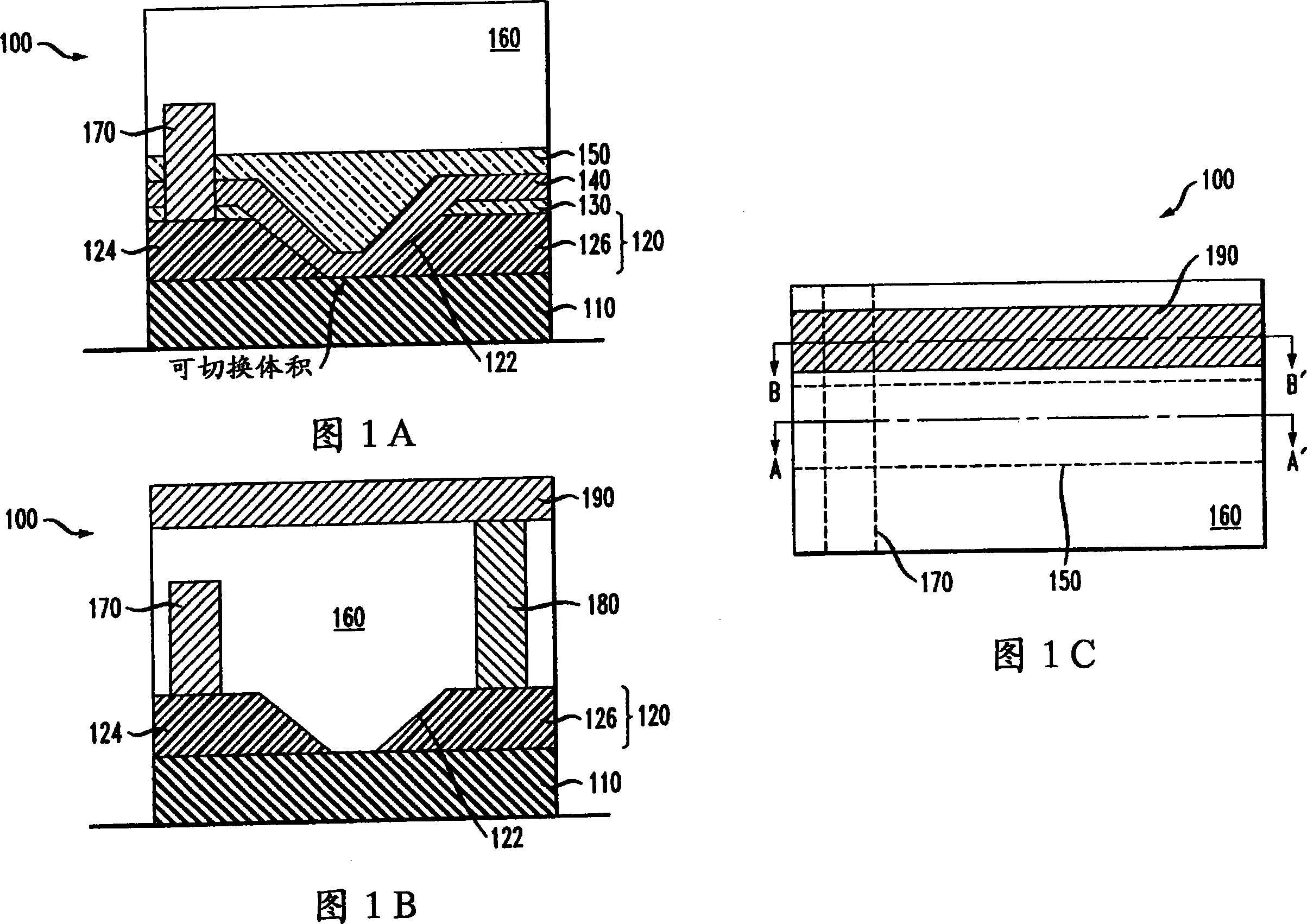
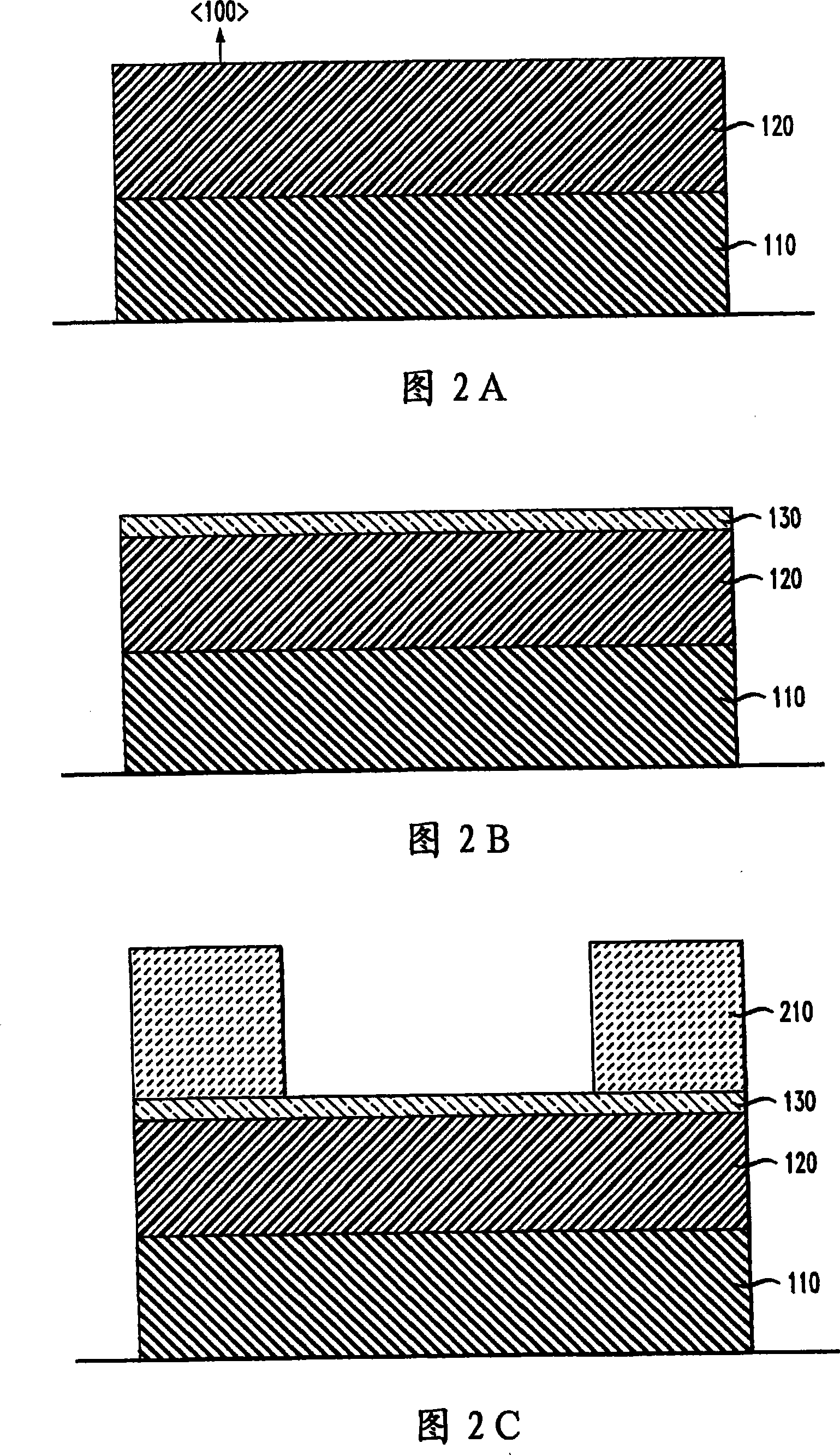
[0016] The invention will be described herein in connection with exemplary memory cells for use in integrated circuits and methods of forming such memory cells. It should be understood, however, that the invention is not limited to the specific materials, features, and processing steps shown and described herein. Modifications to the exemplary embodiments will become apparent to those skilled in the art.

[0017] With regard to processing steps in particular, it should be emphasized that the descriptions provided herein are not intended to encompass all processing steps that may be required to successfully form a functional integrated circuit device. Conversely, certain processing steps commonly used to form integrated circuit devices (eg, wet cleaning and annealing steps) are intentionally not described here for simplicity of illustration. However, those process steps omitted from these general descriptions will readily be appreciated by those skilled in the art. Furthermor...


PUM


Abstract

A memory cell comprises a semiconductor feature and a phase change material. The semiconductor feature defines a groove that divides the semiconductor feature into a first electrode and a second electrode. The phase change material at least partially fills this groove and acts to electrically couple the first and second electrodes. At least a portion of the phase change material is operative to switch between lower and higher electrical resistance states in response to an application of a switching signal to at least one of the first and second electrodes.

Description

technical field [0001] The present invention relates generally to memory cells in integrated circuits, and more particularly to memory cells including phase change materials. Background technique [0002] Recently, as more has been learned about phase change materials (PCMs) and their integration in integrated circuits, the possibility of using these materials in non-volatile memory cells has increased. When incorporated into a memory cell, these materials can be switched between higher and lower resistance states by applying a current pulse ("switching current pulse") to the memory cell. Subsequently, after the memory cell has been written in this manner, the resistance state of a given memory cell can be determined (ie read) by applying a low magnitude read voltage to the material to determine its resistance state. In particular, in some designs, PCM-based memory cells can even store multiple bits of information simultaneously. [0003] Currently, such as doped SbTe and ...

Claims


Application Information

Patent Timeline
Patent Type & Authority Applications(China)
IPC IPC(8): H01L45/00H01L27/24G11C11/56
CPCH01L45/143H01L45/04H01L45/147H01L45/1675H01L27/2436H01L45/146H01L45/06H01L45/144H01L45/148H01L45/1226H01L2924/0002H10B63/30H10N70/823H10N70/231H10N70/20H10N70/8825H10N70/8836H10N70/884H10N70/8828H10N70/8833H10N70/063H01L2924/00
Inventor A·G·施罗特林仲汉M·J·布赖特维施
Owner IBM CORP
Why Eureka
Try Eureka