Making method for semiconductor encapsulation component and semiconductor part location structure and method

A positioning method and semiconductor technology, applied in semiconductor/solid-state device manufacturing, semiconductor/solid-state device components, semiconductor devices, etc., can solve problems such as insufficient filling of glue, slow dispensing speed, and rising costs.

Inactive Publication Date: 2008-03-26
SILICONWARE PRECISION IND CO LTD
View PDF4 Cites 6 Cited by
  • Summary
  • Abstract
  • Description
  • Claims
  • Application Information

AI Technical Summary

Problems solved by technology

[0007] However, in the aforementioned manufacturing method, in order to effectively position the substrate 20 and cover the gap 27, it is disclosed that the gap 27 between the substrate 20 and the carrier 26 is filled with, for example, solder mask (Solder Mask) or The glue 28 of polymer materials such as epoxy resin can speed up the dispensing operation. Usually, the gap 27 needs to be reserved at least 1mm, so that the dispensing operation can be quickly filled in the gap 27 by writing (pen-write). Adhesive material 28, but the larger the gap 27, the more the amount of rubber material 28 required, resulting in an increase in cost; at the same time, if the gap 27 is too large, it is easy to cause the substrate 20 that is pre-bonded on the adhesive tape to shift. It even causes troubles in the subsequent manufacturing method. For example, due to the deviation of the substrate 20, the gaps between the two opposite sides are different, which leads to insufficient filling of the glue on one side, while the glue overflow problem occurs on the other side (as shown in FIG. 4A ), even corresponding to the occurrence of overflow. On one side of the glue, when the encapsulant 23 covering the chip 21 is subsequently formed, the glue 28 (as shown in FIG. 4B ) will remain between the encapsulant 23 and the substrate 20, and the edge delamination problem will easily occur.
Relatively, if the gap 27 is too small, although the problem of substrate 20 offset can be reduced, a thinner dispensing needle and a slower dispensing speed must be used to fully fill the gap 27 with the glue 28 , but this will cause the dispensing speed to be too slow, and at the same time lead to an increase in the cost of the manufacturing method

Method used


Image

  • Making method for semiconductor encapsulation component and semiconductor part location structure and method
  • Making method for semiconductor encapsulation component and semiconductor part location structure and method
  • Making method for semiconductor encapsulation component and semiconductor part location structure and method

Examples


no. 1 example

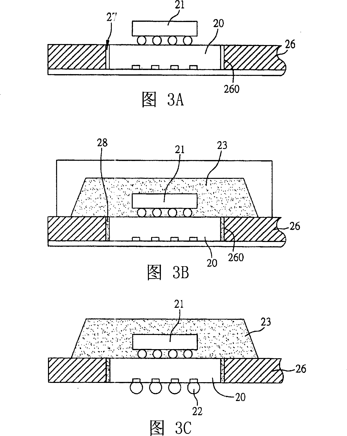
[0066] The preferred embodiment of the semiconductor package manufacturing method proposed by the present invention is shown in FIGS. 5A to 5F. First, as shown in FIGS. 5A and 5B, wherein FIG. 5B is a top view corresponding to FIG. (Build-Up) substrate 30 and carrier 36, the length and width of the substrate 30 can be slightly larger or smaller than the predetermined length and width of the semiconductor package, the carrier 36 has an opening 360, and the length and width of the opening 360 larger than the length and width of the substrate 30 for the substrate 30 carrying the chip 31 to be accommodated in the corresponding opening 360 . The material of the carrier 36 can be an organic insulating material such as FR4, FR5, BT or the like.

[0067] Moreover, at least one storage hole 361 is formed on the periphery of the opening 360 of the carrier 36 . In this figure, storage holes 361 are formed at four corners of the opening 360 of the carrier.

[0068] To accommodate the sub...

no. 2 example

[0080] In addition to selecting organic insulating materials such as FR4, FR5, BT, etc., the carrier of the present invention can also use metal materials coated with a metal coating on the surface. The metal coating is a coating material that is not easy to adhere to the packaging colloid. Its embodiment is shown in Figure 6A As shown in 6D, the content of this embodiment is substantially the same as that of the aforementioned first embodiment, and the main difference is only in the selection of materials for the carrier and some steps of the manufacturing method.

[0081]As shown in FIG. 6A, a build-up substrate 40 and a carrier 46 carrying a chip 41 are prepared, the carrier 46 has an opening 460, and the length and width of the opening 460 are larger than the size of the substrate 46, wherein the carrier 46 A metal material such as copper (Cu) is selected, and the surface of the carrier 46 is pre-plated with a metal coating such as gold (Au), nickel (Ni), chromium (Cr), etc...


PUM


Abstract

This invention relates to a manufacturing method for semiconductor package pieces and a locating structure and a method for semiconductor elements, which provides a base board and a loader for locating said board, in which, the length and width of the board approach to the pre-desinged size of the package piece, a chip is set on the board, an aperture is set on the loader and the size of which is greater than that of the board and at least one storage hole is set around the aperture to hold the board in the aperture, at the same time, glue is filled into the storage hole then to fill the gap between the board and the loader by capillarity and form a package colloid covering said chip then to demold and cut along the edge of the base board according to the pre-designed size of the package piece after the covering area of the colloid is greater than that of the aperture so as to manufacture a semiconductor package piece.

Description

technical field [0001] The invention relates to a semiconductor manufacturing method, in particular to a semiconductor package manufacturing method and a semiconductor element positioning structure and method. Background technique [0002] A molded flip-chip ball grid array (Molded Flip-Chip Ball Grid Array, Molded FCBGA) semiconductor package is shown in FIG. The chip 11, and the plurality of solder balls 12 planted on the lower surface of the substrate 10 to electrically connect to the outside world, and at the same time, the package also includes a molding method formed on the upper surface of the substrate 10 and covering the chip 11 The encapsulation colloid 13. Related prior art such as US Patent No. 6,038,136, No. 6,444,498, No. 6,699,731 or Taiwan Patent Publication No. 559960 have disclosed similar packaging structures. [0003] Regarding the manufacturing method of the molded flip-chip ball grid array semiconductor package, as disclosed in Taiwan Patent Publicati...

Claims


Application Information

Patent Timeline
Patent Type & Authority Applications(China)
IPC IPC(8): H01L21/50H01L21/56H01L21/58H01L23/13H01L23/488H01L23/31
CPCH01L2224/13
Inventor 曾文聪蔡和易黄建屏萧承旭张志伟
Owner SILICONWARE PRECISION IND CO LTD
Why Eureka
Try Eureka