Encapsulation method and structure for OLED device

A technology of light-emitting display and packaging method, which is applied to lighting devices, electroluminescent light sources, light sources, etc., and can solve problems such as short circuits, circuit burnout of organic light-emitting display devices, and wire erosion.

Inactive Publication Date: 2008-04-02
RITDISPLAY
View PDF0 Cites 5 Cited by
  • Summary
  • Abstract
  • Description
  • Claims
  • Application Information

AI Technical Summary

Problems solved by technology

[0007] However, in practical applications, some moisture and oxygen will still penetrate into the packaging structure at the joint between the second sealing layer 160 and the upper cover 150, so that the anode wire 120a or the anode lead 120a The above-mentioned cathode wire 120b is corroded, which causes the circuit of the organic light-emitting display device to be burned or short-circuited.

Method used


Image

  • Encapsulation method and structure for OLED device
  • Encapsulation method and structure for OLED device
  • Encapsulation method and structure for OLED device

Examples


Embodiment Construction

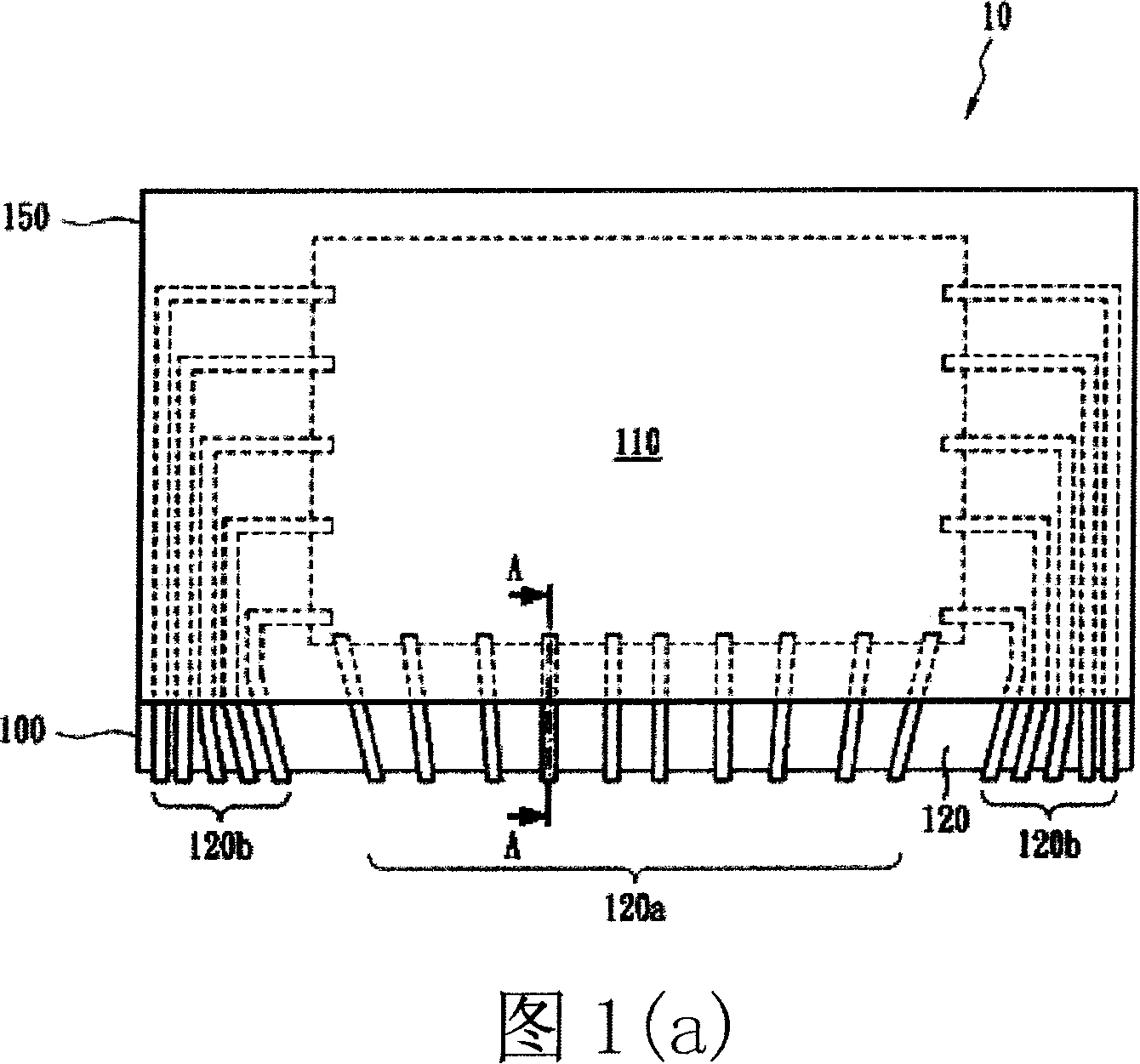
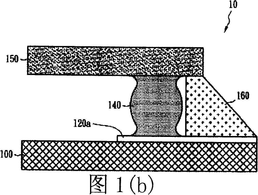
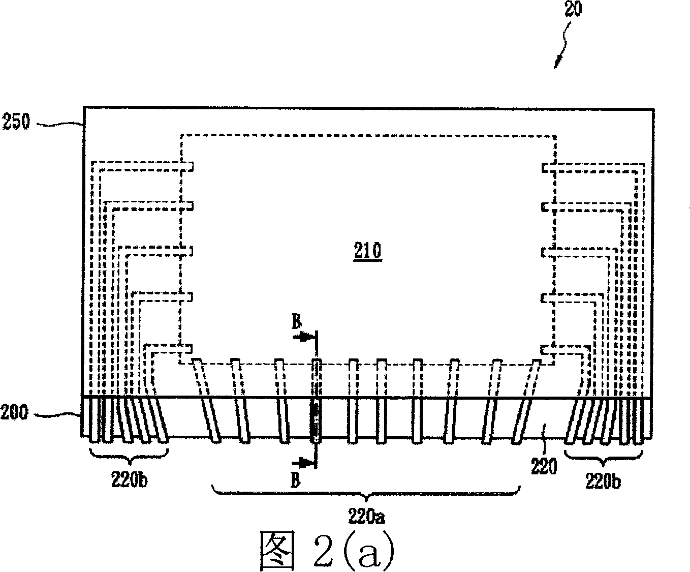
[0058] FIG. 2( a ) is a schematic top view of the organic light emitting display device packaging structure 20 according to the first embodiment of the present invention. The organic light emitting display device packaging structure 20 includes a light emitting region 210 and a wire region 220 formed on a substrate 200 . The light-emitting area 210 contains a plurality of anode lines and a plurality of cathode lines (not shown) stacked on the substrate 200, and the lines in the light-emitting area 210 are sealed in the light-emitting area 210 by the upper cover 250 and the substrate 200. within a space. The wire region 220 includes a plurality of anode wires 220a connected to the anode wires and a plurality of cathode wires 220b connected to the cathode wires, which are respectively stacked on the substrate 200 outside the light emitting region 210 . The anode wires 220 a and the cathode wires 220 b are gathered together on the same side of the substrate 200 .

[0059] Fig. 2...


PUM

PropertyMeasurementUnit
heat deflection temperatureaaaaaaaaaa
thicknessaaaaaaaaaa
thicknessaaaaaaaaaa

Abstract

The present invention reveals a packaging method for organic luminescent display device. The packaging method comprises the following steps: firstly, an insulating material layer is covered on part of a conductor area on a substrate so as to coat an anode conductor or a cathode conductor of the conductor area, wherein, the substrate comprises the conductor area and a luminescent area; then the insulating material layer is covered with a first sealing glue layer; subsequently the first sealing glue layer and the luminescent area are covered with an upper cover body; finally, the insulating material layer of the conductor area and the substrate are covered with a second sealing glue layer. As the insulating material layer coats the clad the anode conductor or the cathode conductor, the present invention can completely prevent the inleak of exterior hydrosphere and oxygen, so as to protect the anode conductor or the cathode conductor of the outer conductor area of the first sealing glue layer from oxidative erosion.

Description

technical field [0001] The present invention relates to a packaging method and structure, in particular to a packaging method and structure of an organic light emitting display device (Organic Light Emitting Device; OLED). Background technique [0002] At present, the common technology of organic light-emitting display devices is to apply Chip on Film (COF) components to connect with the glass substrate of the display. This technology is to directly bond the driver IC to the film. COF is a kind of driver IC. Flip Chip Bonding (Flip Chip Bonding) technology on the flexible printed circuit (Flexible Printed Circuit; FPC) board substrate, that is, the driver IC and its electronic components can be directly fixed on the film, which can save the traditional printing circuit board, and achieve the purpose of being lighter, thinner and shorter. [0003] Another common technology of organic light-emitting display devices is to apply chip on glass (Chip on Glass; COG) technology to ...

Claims


Application Information

Patent Timeline
Patent Type & Authority Applications(China)
IPC IPC(8): H01L21/50H01L21/56H01L27/32H01L51/56H01L51/50H01L51/52H05B33/10H05B33/12H05B33/04
Inventor 廖孟杰邹忠哲
Owner RITDISPLAY
Why Eureka
Try Eureka