Epitaxial structure of semiconductor and growth method of epitaxial structure

A technology of epitaxial structure and growth method, which is applied in semiconductor/solid-state device manufacturing, electrical components, circuits, etc., can solve problems such as device performance impact, achieve stress regulation, save time, and avoid the effect of crystal quality degradation

Active Publication Date: 2013-01-02
ENKRIS SEMICON
View PDF5 Cites 12 Cited by
  • Summary
  • Abstract
  • Description
  • Claims
  • Application Information

AI Technical Summary

Problems solved by technology

These defects can have fatal effec

Method used


Image

  • Epitaxial structure of semiconductor and growth method of epitaxial structure
  • Epitaxial structure of semiconductor and growth method of epitaxial structure
  • Epitaxial structure of semiconductor and growth method of epitaxial structure

Examples


Embodiment Construction

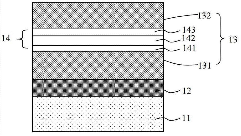
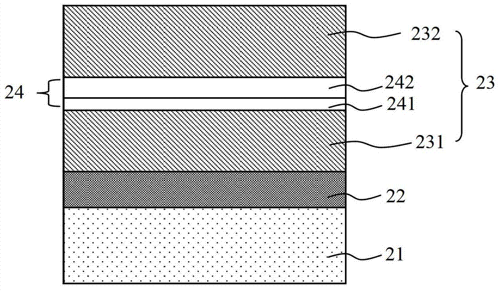
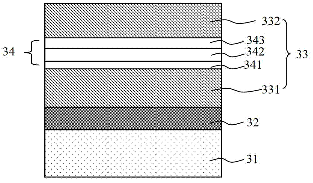
[0039] The embodiment of the present invention discloses a semiconductor epitaxial structure, including:

[0040] a nitride nucleation layer formed on a silicon or silicon carbide substrate;

[0041] a nitride layer formed on the nitride nucleation layer, the nitride layer comprising a first nitride layer and a second nitride layer;

[0042] an insertion layer between the first nitride layer and the second nitride layer, the insertion layer includes a first insertion layer and a second insertion layer above the first insertion layer, the first insertion layer The first insertion layer is an aluminum gallium nitride layer, the second insertion layer is an aluminum gallium nitride layer or an aluminum nitride layer, and the average content of aluminum in the first insertion layer is lower than the average content of aluminum in the second insertion layer.

[0043] Correspondingly, the embodiment of the present invention also discloses a method for growing a semiconductor epitax...


PUM

PropertyMeasurementUnit
Thicknessaaaaaaaaaa
Temperatureaaaaaaaaaa

Abstract

The invention discloses an epitaxial structure of a semiconductor. The epitaxial structure of the semiconductor comprises a nitride nucleating layer formed on a silicon or silicon carbide substrate, a nitride layer on the nitride nucleating layer and an insertion layer inside the nitride layer. The insertion layer comprises a first insertion layer and a second insertion layer placed above the first insertion layer, the first insertion layer is an aluminum gallium nitrogen layer, the second insertion layer is an aluminum gallium nitrogen layer or an aluminum nitride layer, and the average content of aluminum in the first insertion layer is lower than the average content of aluminum in the second insertion layer. The invention also discloses a growth method of the epitaxial structure of the semiconductor. According to the epitaxial structure of the semiconductor disclosed by the invention, the crystal quality can be prevented from dropping when compressive stress is being applied, and a cracking effect or drop of the surface quality possibly caused by the temperature variation can be avoided. In addition, the whole epitaxial layer grows at a high temperature, so that repeated cooling and heating operations are not needed, and the complexity of the process can be reduced.

Description

technical field [0001] The invention belongs to the technical field of semiconductors, and in particular relates to a semiconductor epitaxial structure and a growth method thereof. Background technique [0002] Gallium Nitride, the third-generation wide bandgap semiconductor material, has the characteristics of large bandgap, high electron saturation drift velocity, high breakdown field strength, and good thermal conductivity. high frequency, high voltage and high power devices. Gallium nitride devices have good application prospects in high-frequency and high-power microwave devices. Since the 1990s, the development of gallium nitride devices has been one of the hot spots in the research of electronic devices. Due to the lack of GaN intrinsic substrates, GaN devices are fabricated on heterogeneous substrates, such as sapphire, SiC and Si. Among these types of substrates, the silicon substrate has the largest size (200mm) and the lowest price, so growing gallium nitride ma...

Claims


Application Information

Patent Timeline
IPC IPC(8): H01L21/02
Inventor 程凯
Owner ENKRIS SEMICON
Why Eureka
Try Eureka