Vertical conduction gallium nitride power diode and preparation method thereof
A technology of power diodes and gallium nitride, which is applied in the direction of diodes, semiconductor/solid-state device manufacturing, semiconductor devices, etc., can solve the problems of limiting current vertical conduction and non-adjustable stress, so as to improve device performance and withstand voltage performance Effect
- Summary
- Abstract
- Description
- Claims
- Application Information
AI Technical Summary
Problems solved by technology
Method used
Image
Examples
Embodiment 1
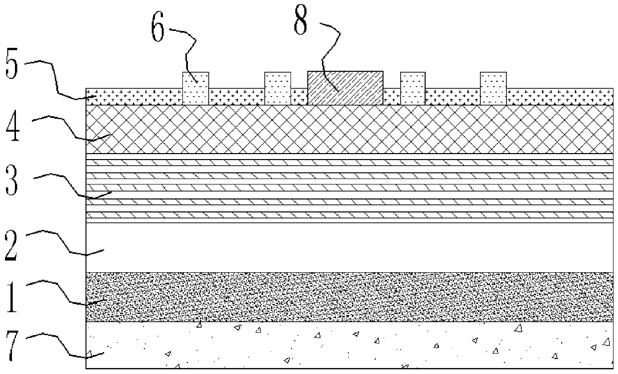
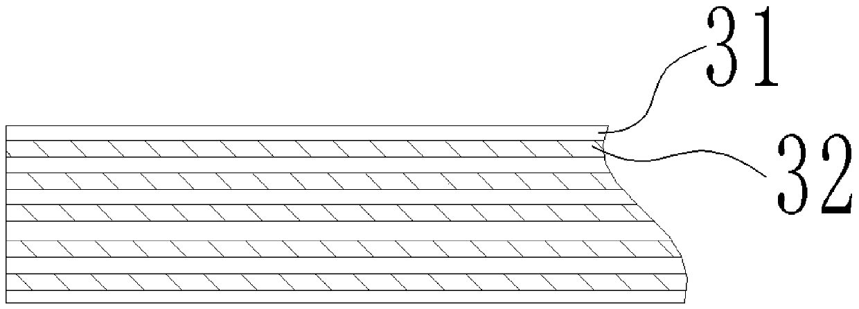
[0054] Such as figure 1 and image 3As shown, a vertical conduction gallium nitride power diode, the epitaxy of the diode includes a substrate 1, and a nucleation layer 2, a superlattice stress buffer layer 3, a GaN Drift layer 4, mask layer 5; substrate 1, nucleation layer 2, superlattice stress buffer layer 3, GaN drift layer 4, mask layer 5 together constitute the epitaxial growth part of the diode, substrate 1 and GaN drift layer 4 is also provided with a first electrode 7 and a second electrode 8 with different electrical contacts by means of deposition, preferably, the first electrode 7 is a cathode, and the second electrode 8 is an anode.
[0055] The substrate 1 is a silicon substrate with low resistance, and the silicon substrate is used, and its cost is lower than that of substrates made of other materials;
[0056] The superlattice stress buffer layer 3 is an AlN / GaN superlattice, the thickness of the superlattice stress buffer layer 3 is 0.1nm-100nm, and the AlN / ...
Embodiment 2
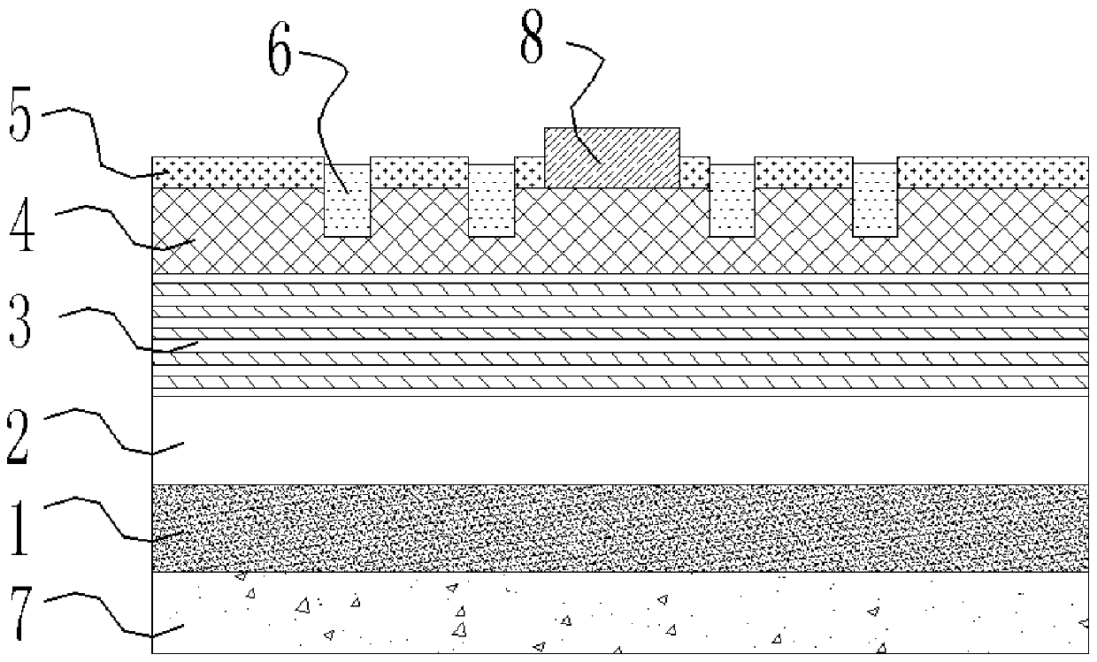
[0077] This embodiment is another embodiment of the diode of the vertical conductor in Embodiment 1, such as figure 2 As shown, in this embodiment, the first groove 51 provided on the mask layer 5 also cuts into the inside of the GaN drift layer 4 but does not penetrate the GaN drift layer 4, so that the field limiting ring 6 and the GaN drift The contact area of the layer 4 is larger, which can better conduct the contact with the GaN drift layer 4, so that the breakdown voltage can be further improved.
[0078] It should be pointed out that the first groove 51 mentioned here is cut into the inside of the GaN drift layer 4, which means that the first groove is etched in the mask layer 5 by photolithography and development technology and wet etching method. A groove continues to be etched in the GaN drift layer 4 after penetrating the mask layer 5 , thereby achieving the effect of cutting the first groove 51 into the GaN drift layer 4 .
[0079] and, if Figure 4 to Figure...
PUM
| Property | Measurement | Unit |
|---|---|---|
| Thickness | aaaaa | aaaaa |
| Thickness | aaaaa | aaaaa |
| Growth thickness | aaaaa | aaaaa |
Abstract
Description
Claims
Application Information


