Liquid crystal display board and method for manufacturing facing direction substrates thereof

A liquid crystal display panel and facing substrate technology, which is applied in the direction of optics, instruments, electrical components, etc., can solve the problems of different height differences, spherical gaps that cannot provide uniformity, and difficult to maintain the optical characteristics of the panel, etc.

Active Publication Date: 2008-04-16
AU OPTRONICS CORP
View PDF0 Cites 20 Cited by
  • Summary
  • Abstract
  • Description
  • Claims
  • Application Information

AI Technical Summary

Problems solved by technology

[0004] However, it is worth noting that ball spacers are traditionally used in this type of liquid crystal display panel. Since it is not easy to control the position of the ball spacers during spreading, the ball spacers are prone to fluctuations due to the fluctuation of the surface of the thin film transistor array substrate. , resulting in the formation of different height differences, resulting in the inability of the spherical spacer to provide a uniform liquid crystal gap (cellgap) between the thin film transistor array substrate and the opposite substrate
Therefore, when this kind of liquid crystal display panel is squeezed by external force, it is difficult to maintain the distance between the thin film transistor array substrate with the color filter layer and the opposite substrate, which will affect the optical characteristics of the panel, resulting in uneven display of the panel.

Method used


Image

  • Liquid crystal display board and method for manufacturing facing direction substrates thereof
  • Liquid crystal display board and method for manufacturing facing direction substrates thereof
  • Liquid crystal display board and method for manufacturing facing direction substrates thereof

Examples


Embodiment Construction

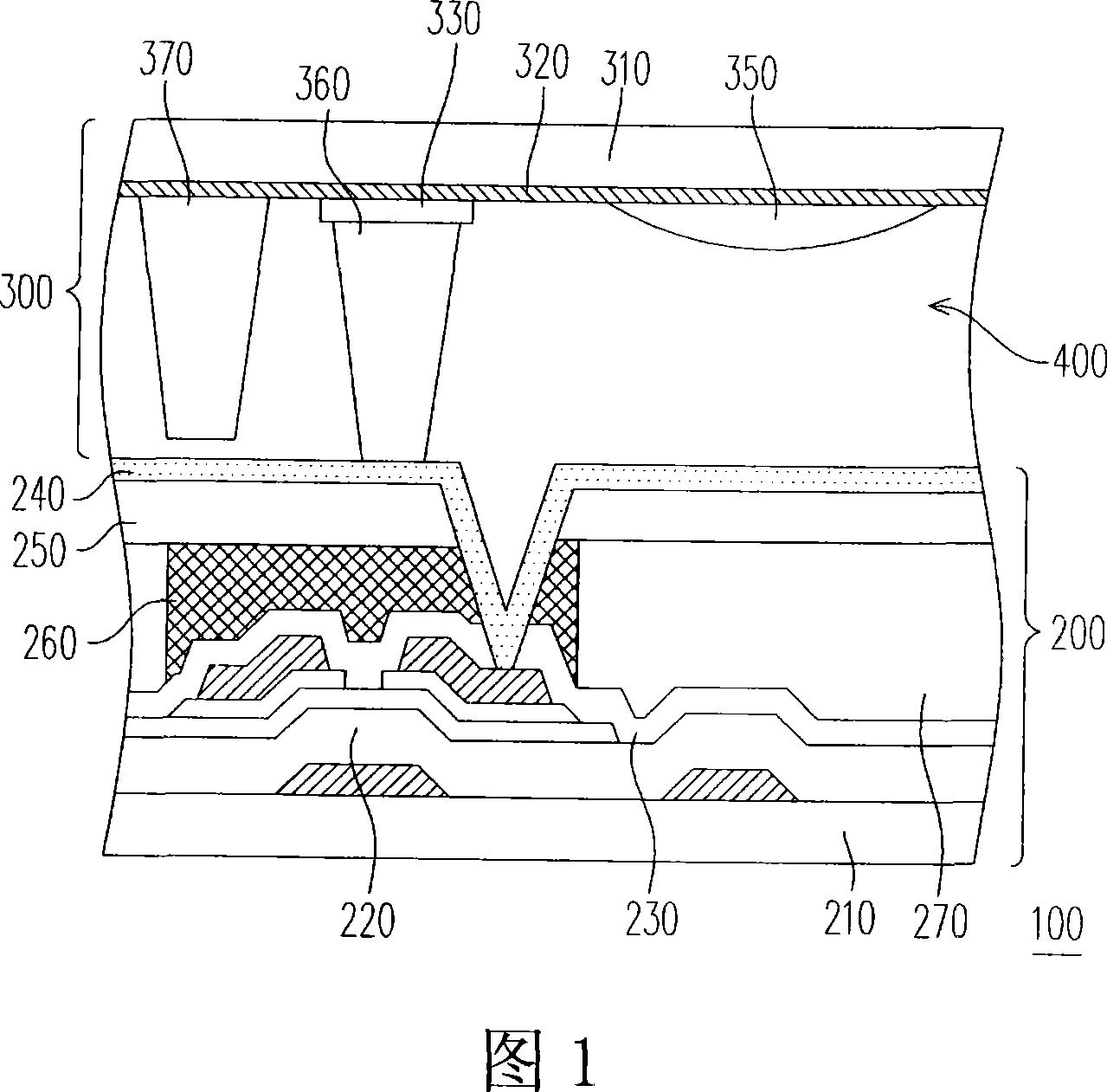
[0040]FIG. 1 is a schematic structural diagram of a liquid crystal display panel according to an embodiment of the present invention. Please refer to FIG. 1 first. The liquid crystal display panel 100 includes a thin film transistor array substrate (colorfilter on array (COA) substrate) 200 with a color filter layer, a pair of opposite substrates (opposite substrate) 300 and a color filter. A liquid crystal layer 400 between the thin film transistor array substrate 200 and the opposite substrate 300 .

[0041] The thin film transistor array substrate 200 with a color filter layer includes a substrate 210, a plurality of scanning lines (not shown), a plurality of data lines (not shown), a plurality of thin film transistors 220, a plurality of color filter layers 230 and a plurality of pixel electrodes 240 . Scanning lines, data lines and thin film transistors 220 are all arranged on the substrate 210, and the scanning lines and data lines are staggered to form pixel areas arra...


PUM


Abstract

The invention discloses a liquid crystal display panel and a manufacturing method of an opposite base plate. The liquid crystal display panel comprises a thin film transistor array base plate with a colorful filter layer, the opposite base plate and a liquid crystal layer. The opposite base plate is provided with a common electrode, a plurality of main gap objects arranged on the common electrode, a plurality of gap object seats which are arranged on the common electrode and bulge toward the thin film transistor array base plate with the colorful filter layer, and a plurality of sub gap objects arranged on the common electrode. The main gap objects are arranged on the gap object seats for maintaining gaps between the thin film transistor array base plate with the colorful filter layer and the opposite base plate. The liquid crystal layer is also arranged between the thin film transistor array base plate with the colorful filter layer and the opposite base plate. Due to the main gap objects and the sub gap objects, the liquid crystal display panel of the invention forms a liquid crystal display panel with mixed type gap objects.

Description

technical field [0001] The present invention relates to a liquid crystal display panel (liquid crystal display panel, LCD panel) and a method for manufacturing its opposite substrate (opposite substrate), in particular to a liquid crystal display panel with a hybrid design spacer (hybrid spacer) And the method of manufacturing its opposite substrate. Background technique [0002] Liquid crystal displays have the advantages of high image quality, small size, light weight, low voltage drive, low power consumption, and wide application range. Therefore, they have replaced cathode ray tubes (CRTs) and become the mainstream of the new generation of displays. A conventional liquid crystal display panel is composed of a color filter substrate (color filter), a thin film transistor array substrate (thin film transistor array substrate, TFT array substrate), and a liquid crystal layer disposed between the two substrates. However, the resolution of this liquid crystal display panel i...

Claims


Application Information

Patent Timeline
Patent Type & Authority Applications(China)
IPC IPC(8): G02F1/1362G02F1/1335G02F1/1339G02F1/1343G02F1/1333H01L27/12H01L23/544
Inventor 黄彦衡陈宗凯李淑琴
Owner AU OPTRONICS CORP
Why Eureka
Try Eureka