Optical backplane connector, photoelectric conversion module and optical backplane
A technology for photoelectric conversion modules and optical connectors, applied in the directions of light guides, optics, instruments, etc., can solve the problems of circuit board transmission rate hindering equipment capacity improvement, etc., to improve maintainability, facilitate component layout, and improve component installation density. Effect
- Summary
- Abstract
- Description
- Claims
- Application Information
AI Technical Summary
Problems solved by technology
Method used
Image
Examples
no. 1 example
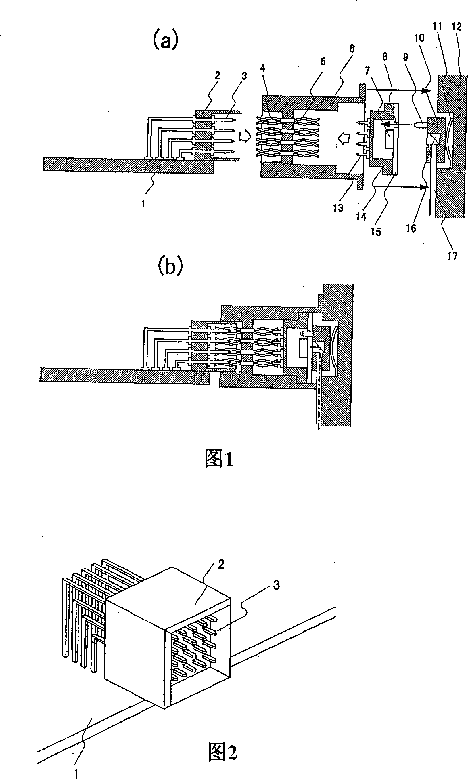
[0075] Fig. 1 (a), (b) shows the optical backplane connector and the optical backplane according to the first embodiment of the present invention. FIG. 1( a ) is a sectional view showing a connection operation between a board and an optical backplane and an assembly and installation operation of an optical backplane connector, and FIG. 1( b ) is a sectional view showing a connection state.
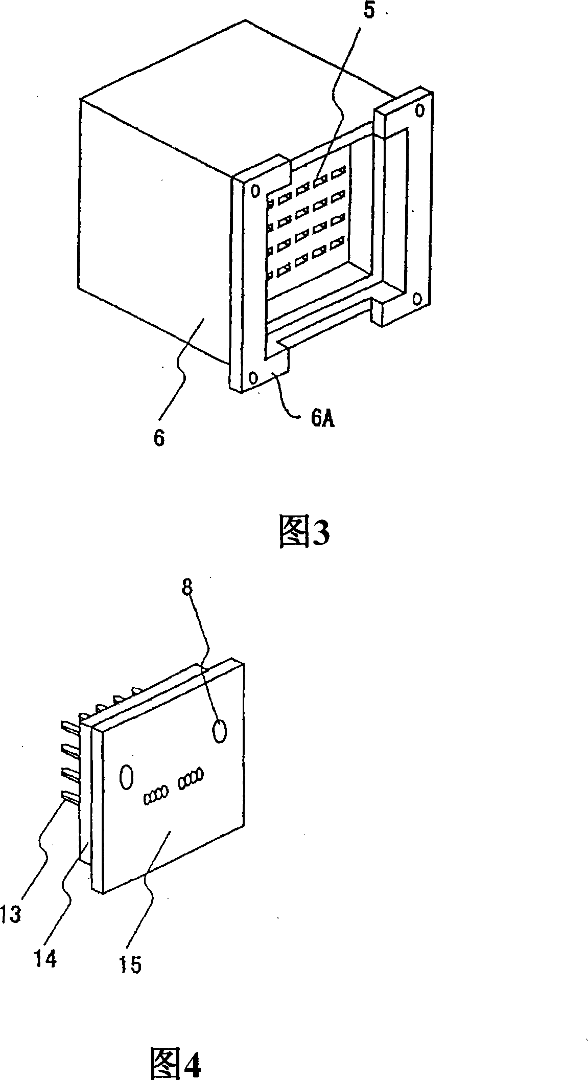
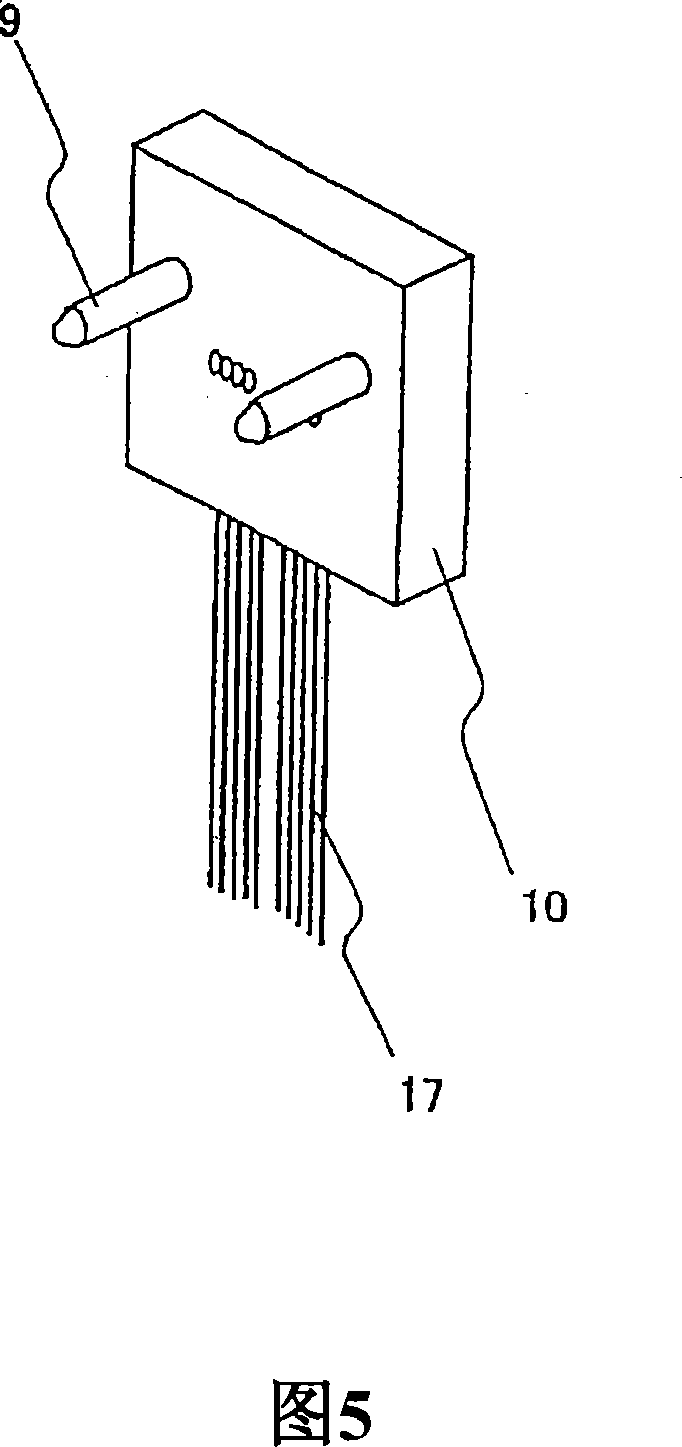
[0076] 2 is a perspective view showing the electrical connector on the board side, FIG. 3 is a perspective view of the optical backplane connector viewed from the side of the photoelectric conversion module, FIG. 4 is a perspective view of the photoelectric conversion module viewed from the side of the backplane, and FIG. 5 is a perspective view showing the optical connector 10, and FIG. 6 is a perspective view showing a part of the optical backplane.
[0077] FIG. 7 is an assembly diagram of the board-side electrical connector, the optical backplane connector and the photoelectric convers...
no. 2 example
[0089] Fig. 9 shows an optical backplane connector and an optical backplane according to a second embodiment of the present invention. In FIG. 9, the same elements as those in FIG. 1 are respectively denoted by the same reference numerals without further explanation. The photoelectric conversion module 14 accommodates a plurality of photoelectric conversion elements 7 coupled to light transmission paths 17 extending in different directions. Fitting holes 8 of the photoelectric conversion modules 6 are formed between the photoelectric conversion elements 7 , and guide pins 9 of the optical connector 10 are inserted into the fitting holes 8 . According to this embodiment, the switch board installed near the center of the rack can be connected to each of the right and left connected to the signal input / output board. In FIG. 9 , for ease of understanding, the case where two optical transmission paths 17 are included is exemplified. However, three or more optical transmission pa...
no. 3 example
[0091] Fig. 10 shows an optical backplane connector and an optical backplane according to a third embodiment of the present invention. Fig. 10(a) is an exploded sectional view showing this structure viewed from the upper surface of the board, and Fig. 10(b) is a sectional view viewed from the upper surface of the board inserted into the backplane. And, FIG. 11 is a diagram showing a method of fixing the optical connector and the cover. In Fig. 10(a), (b), the same elements as in Fig. 1 are respectively indicated by the same reference numerals without further explanation.
[0092] According to the present embodiment, the cover 20 is arranged on the through hole through which the light backplane of the backplane passes. By opening the cover 20 and pulling out the guide pin 9 of the optical connector 10 from the mating hole 8 of the photoelectric conversion module 14, the photoelectric conversion module can be taken out to the back of the optical backplane. Due to this structure,...
PUM
 Abstract
Description
Claims
Application Information


