Built-in testing realization method of circuit board interconnect fault under boundary scanning environment

A technology of boundary scan and built-in testing, applied in digital circuit testing, electronic circuit testing, electrical measurement, etc., can solve the problem of test response diversity and disordered response analyzer 3', which is inconvenient to design, test incentives are not uniform, and increase Response analyzer 3'hardware overhead and other issues

Inactive Publication Date: 2008-05-21
BEIHANG UNIV
View PDF0 Cites 11 Cited by
  • Summary
  • Abstract
  • Description
  • Claims
  • Application Information

AI Technical Summary

Problems solved by technology

However, in the above two documents, the receiving unit is classified into the driving unit (collectively referred to as the data unit), and the test stimulus is allocated to them in the same way. , cannot be loaded onto the interconnection network during the test and has no effect, thus causing additional hardware overhead for the test generator 1'
[0009] (2) The test stimuli loaded on the same interconnection network are not uniform
In Document 2 and Document 3, all the drive units are sorte

Method used


Image

  • Built-in testing realization method of circuit board interconnect fault under boundary scanning environment
  • Built-in testing realization method of circuit board interconnect fault under boundary scanning environment

Examples


Embodiment Construction

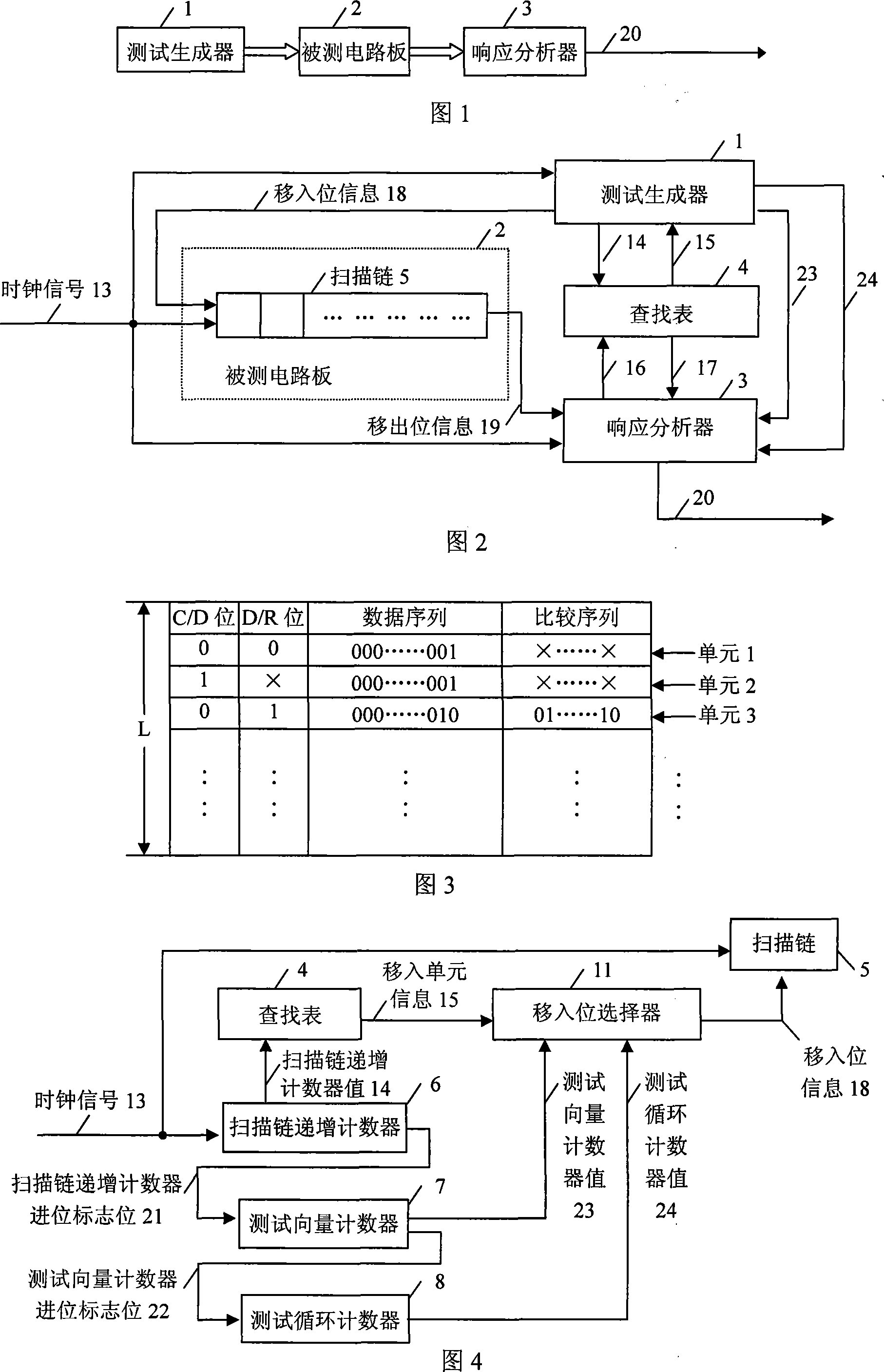
[0104] The specific embodiments of the present invention will be further described in detail below in conjunction with the accompanying drawings.

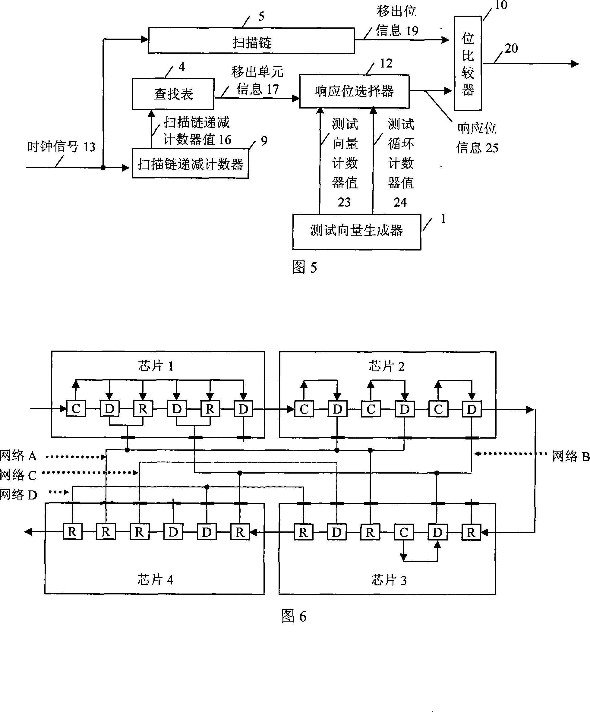
[0105] FIG. 6 is a simplified schematic diagram of the interconnection network of a circuit board 2 under test. The scan chain 5 of this circuit board includes 24 boundary scan units (these 24 scan units are respectively named "unit 1", "unit 2", ..., "unit 24" according to the flow direction of the arrow). "C" in the figure indicates the control unit, "D" indicates the drive unit, and "R" indicates the receiver unit; if the drive unit and the receiver unit share the same pin, it indicates a bidirectional unit, for example, "unit 2" and "unit 3" indicate A bi-directional unit; the arrow on the control unit indicates which drive unit or bi-directional unit it controls, e.g. "Unit 1" controls "Unit 2", "Unit 3", "Unit 4", "Unit 5" and "Unit 6 ".

[0106] The overall design of the hardware part of the present invention is shown in F...


PUM


Abstract

The invention relates to a built-in test implementation method for circuit board interconnection faults in a boundary scan environment. The improved counting sequence algorithm and the single enable method are used as the test generation algorithms for the drive unit and the control unit respectively. The overall design of the invention is mainly composed of search Table, Test Generator and Response Analyzer are composed of three parts. This method can achieve 100% fault detection rate for all interconnection faults, including short circuit, open circuit and sluggish fault; it can avoid the problem of multi-driver conflict, so that the test can be carried out safely; and the design process is simple and easy for engineering implementation; in addition, it It also has the advantages of high reliability, fast test speed, and small hardware overhead.

Description

(1) Technical field: [0001] The invention relates to a method for realizing a built-in test (Built InTest, "BIT" for short) of circuit board interconnection faults in a boundary scan environment, and belongs to the technical field of fault detection in the process of circuit board production and maintenance. (two) background technology: [0002] Interconnect testing is a very important issue during the production and maintenance of circuit boards. For example, during the assembly process, faults such as short circuits, sluggishness, and open circuits are easily caused due to inaccurate positioning, poor solder volume control, improper temperature and time control, and other reasons. According to statistics, the number of faults on the interconnect line has accounted for more than half of the faults of the entire circuit board, and with the further improvement of the integration and complexity of the circuit board, this proportion will continue to rise. On the other hand, th...

Claims


Application Information

Patent Timeline
IPC IPC(8): G01R31/02G01R31/28G01R31/317G01R31/3185
Inventor 孟晓风钟波
Owner BEIHANG UNIV
Why Eureka
Try Eureka