High power semiconductor laser device reliability detection method

A laser and high-power technology, applied in semiconductor lasers, single semiconductor device testing, lasers, etc., can solve problems such as loss, reduced service life, and expensive array lasers

Inactive Publication Date: 2008-05-21
JILIN UNIV
View PDF0 Cites 26 Cited by
  • Summary
  • Abstract
  • Description
  • Claims
  • Application Information

AI Technical Summary

Problems solved by technology

In addition, array lasers are expensive, and electrical aging will inevitably reduce their service life. If there is a serious impact loss

Method used


Image

  • High power semiconductor laser device reliability detection method
  • High power semiconductor laser device reliability detection method
  • High power semiconductor laser device reliability detection method

Examples


Embodiment 1

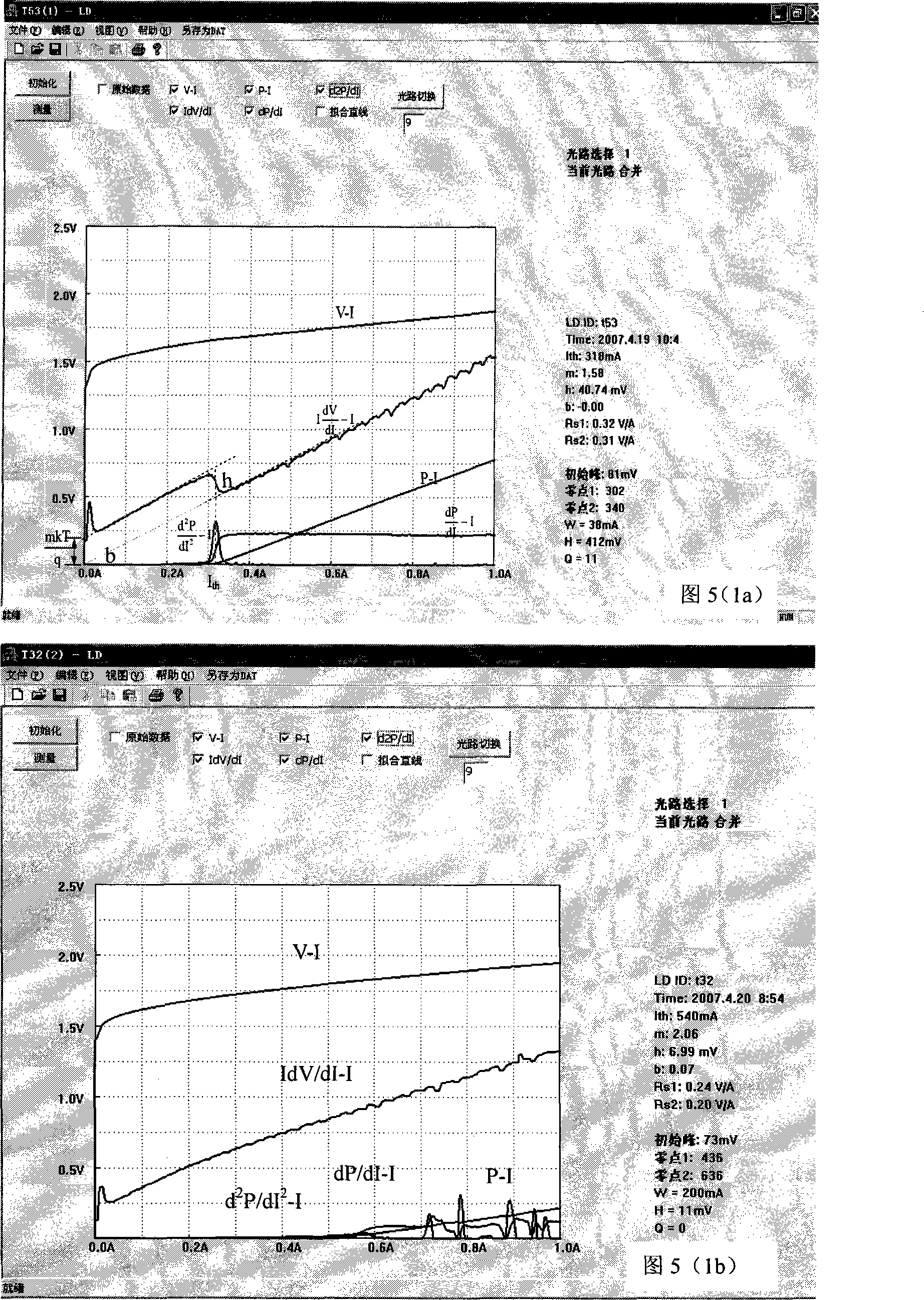
[0092] Example 1: Testing a single-tube high-power laser

[0093]The rated output optical power of the two single-tube high-power 808nm quantum well lasers manufactured by the Changchun Institute of Optics, Mechanics and Physics we measured is CW1W. Using the method described in this patent, the maximum test current value is set to 1A, the step current is 2mA, and the light derivative curve d is used. 2 P / dI 2 ~I judgment threshold, the measured curves are shown in Fig. 5(1a) and Fig. 5(1b).

[0094] The parameters they provide are shown in Table 1:

[0095] Table 1: Parameters of two single-tube high-power 808nm quantum well lasers used in this patent:

[0096] LD No.

Po(W)

Ith(A)

Io(A)

Vo(V)

Es(W / A)

Ep(%)

Rd(Ω)

t53

1.01

0.30

1.50

1.86

0.85

36

0.14

t32

0.26

0.30

1.50

1.91

0.22

9.0

0.09

[0097] Ou...

Embodiment 2

[0102] Example 2: Testing Array High Power Lasers

[0103] The rated output optical power of the two high-power 808nm quantum well array lasers we measured is CW20W, and one of them has experienced power degradation due to use for a period of time. Using the method described in this patent, the maximum test current value is set to 8A , Step current 16mA, using light derivative curve d 2 P / dI 2 ~I judgment threshold, each measured curve is shown in Fig. 5(2a) and Fig. 5(2b).

[0104] The original measurement data provided by them are shown in Table 3:

[0105] Table 3: Parameters of two high power 808nm quantum well array lasers:

[0106] LD No.

Po(W)

Ith(A)

Io(A)

Vo(V)

Es(W / A)

Ep(%)

Rd(Ω)

bz-38

21.3

4.0

25.0

1.65

1.01

51.6

6.6

031233-163

8.5

-

25.0

2.02

0.15

16.9

22.1

[0107] Our test results are shown in Table 4...


PUM


Abstract

The present invention belongs to a detection and analysis method, in particular to a detection and selection method for the quality and reliability of a high power semiconductor laser and an array laser. Firstly, a V-I curve and a P-I curve of the laser are measured; an electrical derivative curve IdV/dI-I and a light derivative curve dP/dI-I and d<2>P/dI<2>-I are obtained through computer processing. Then the threshold current Ith of the measured device is obtained from the light derivative curve d<2>P/dI<2>-I or the electrical derivative curve IdV/dI-I. So the parameters of b, m, Rs1, Rs2 and h are obtained. A light characteristic when the laser is lased is given from a peak height H, a peak width W and a peak height-width ratio O at the threshold of the second order light derivative curve. Finally, the obtained parameters are compared with the normal value of parameters of the device same structure to judge the quality and reliability of the detected high power semiconductor laser or the array laser. The device filtration of the present invention is characterized by no-wear, high-speed and convenience, which is suitable for wide application.

Description

technical field [0001] The invention belongs to the field of laser detection and analysis, and in particular relates to a method for detecting and screening the quality and reliability of high-power semiconductor lasers and array lasers. Background technique [0002] The existing semiconductor laser reliability detection method is to use the electrical aging method to accelerate the aging for a certain period of time (such as 24 hours or longer) when the temperature is increased and the current is increased. By measuring the threshold current or output optical power Devices with large changes before and after aging are screened out to determine the reliability of the device. This method is time-consuming, power-consuming, and an aging station with sufficient capacity is required. For high-power array lasers, the driving current is generally more than tens of amperes, and the burn-in station must have a larger current capacity. In addition, array lasers are expensive, and e...

Claims


Application Information

Patent Timeline
Patent Type & Authority Applications(China)
IPC IPC(8): G01R31/26H01S5/00G01M11/00G01R31/00
Inventor 石家纬郭树旭梁庆成曹军胜刘奎学李红岩
Owner JILIN UNIV
Why Eureka
Try Eureka