


Quick Research
Generate reliable direction feasibility study reports for your R&D in just a few steps.

Technical Q&A
Discover and master advanced knowledge NOW. Basics, ideas, possibilities, all at once.

Find Solutions
As an expert in R&D theories, this can generate solutions to your technical problems instantly.

Evaluate Feasibility
Analyze your overall solution with one click, know your potential R&D risks in advance.

Monitor Landscape
Get weekly tech updates, stay abreast of the latest tech innovations and key insights.
Semiconductor light-emitting device and method of manufacturing the same
一种发光元件、半导体的技术,应用在半导体器件、电气元件、电路等方向,能够解决光取出效果降低等问题,达到缩短距离、提高可靠性的效果
- Summary
- Abstract
- Description
- Claims
- Application Information
AI Technical Summary
Problems solved by technology
Method used
Image

Examples
no. 1 example
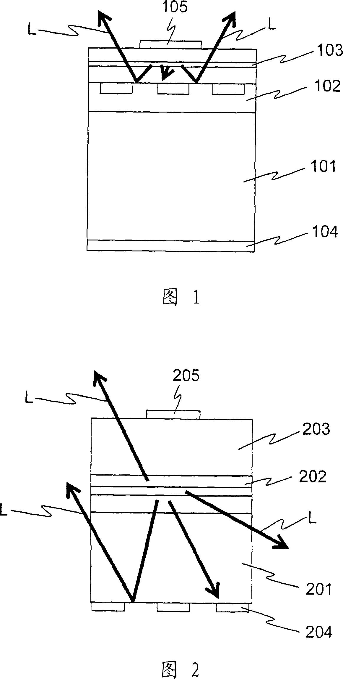
[0133] Fig. 14 is a schematic cross-sectional view showing a semiconductor light emitting element according to a first embodiment of the present invention.
[0134] The above-mentioned semiconductor light-emitting element has: n-type DBR layer 3, n-type Al 0.5 In0.5 P cladding layer 4, quaternary AlGaInP active layer 5, p-type Al 0.5 In 0.5 P cladding layer 6 , p-type GaInP intermediate layer 7 , p-type GaP contact layer 8 , p-type GaP transparent substrate 9 , ohmic electrodes 10 , 11 and reflective layer 12 .
[0135] The above n-type DBR layer 3 consists of 20 pairs of n-type AlAs light reflection layers and n-type Al 0.6 1Ga 0.39 As light reflective layer. In addition, the n-type DBR layer 3 has reflectivity with respect to the emission wavelength of the AlGaInP active layer 5 .
[0136] The above-mentioned AlGaInP active layer 5 emits red light. In addition, the above-mentioned AlGaInP active layer 5 has a quantum well structure. In more detail, the above-mentioned...
no. 2 example
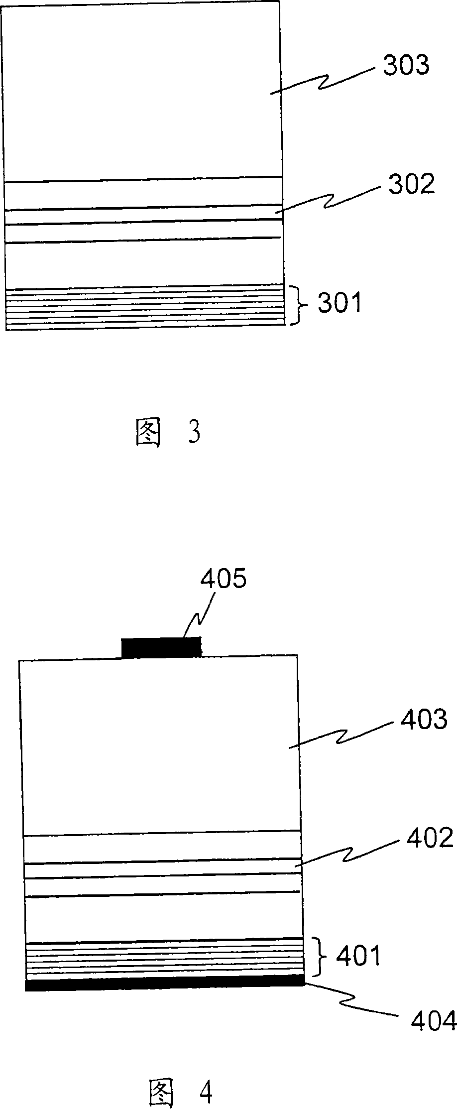
[0172] With respect to the first embodiment described above, the second embodiment is an embodiment in which a support substrate is pasted on the DBR layer via metal.
[0173] Fig. 16 is a schematic cross-sectional view of a semiconductor light emitting element according to a second embodiment of the present invention.
[0174] Semiconductor light-emitting elements have: n-type Al 0.6 Ga 0.4 As current diffusion layer 23, n-type Al 0.5 In 0.5 P cladding layer 24, AlGaInP active layer 25, p-type Al 0.5 In 0.5 P cladding layer 26 , p-type DBR layer 27 , p-type AlGaAs contact layer 28 , ohmic electrodes 29 , 35 , 36 , reflection layer 30 and p-type Si substrate 34 .
[0175] The above-mentioned AlGaInP active layer 25 emits red light. In addition, the above-mentioned AlGaInP active layer 25 has a quantum well structure. In more detail, the above-mentioned AlGaInP active layer 25 is stacked alternately (Al 0.05 Ga 0.95 ) 0.5 In 0.5 P well layer and (Al 0.50 Ga 0.50 ) ...
PUM
 Abstract
Description
Claims
Application Information
 - R&D Engineer
- R&D Manager
- IP Professional
- Industry Leading Data Capabilities
- Powerful AI technology
- Patent DNA Extraction
Browse by: Latest US Patents, China's latest patents, Technical Efficacy Thesaurus, Application Domain, Technology Topic, Popular Technical Reports.
© 2024 PatSnap. All rights reserved.Legal|Privacy policy|Modern Slavery Act Transparency Statement|Sitemap|About US| Contact US: help@patsnap.com