

Forming method of L-shaped side wall
A sidewall, L-shaped technology, used in electrical components, semiconductor/solid-state device manufacturing, semiconductor devices, etc., can solve problems such as substrate surface damage, and achieve the effect of improving uniformity and preventing damage.
- Summary
- Abstract
- Description
- Claims
- Application Information
AI Technical Summary
Problems solved by technology
Method used
Image

Examples
Embodiment Construction
[0020] In order to make the purpose and features of the present invention more comprehensible, the specific implementation manners of the present invention will be further described below in conjunction with the accompanying drawings.
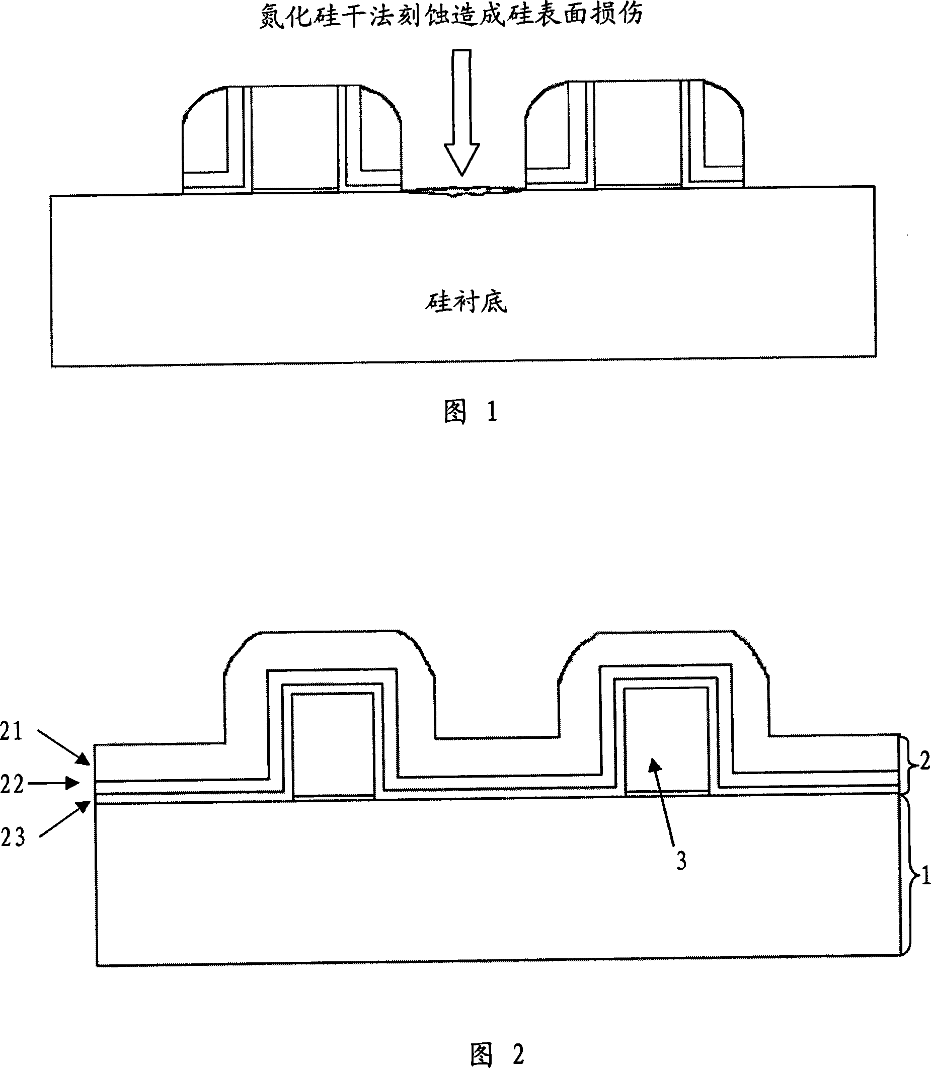
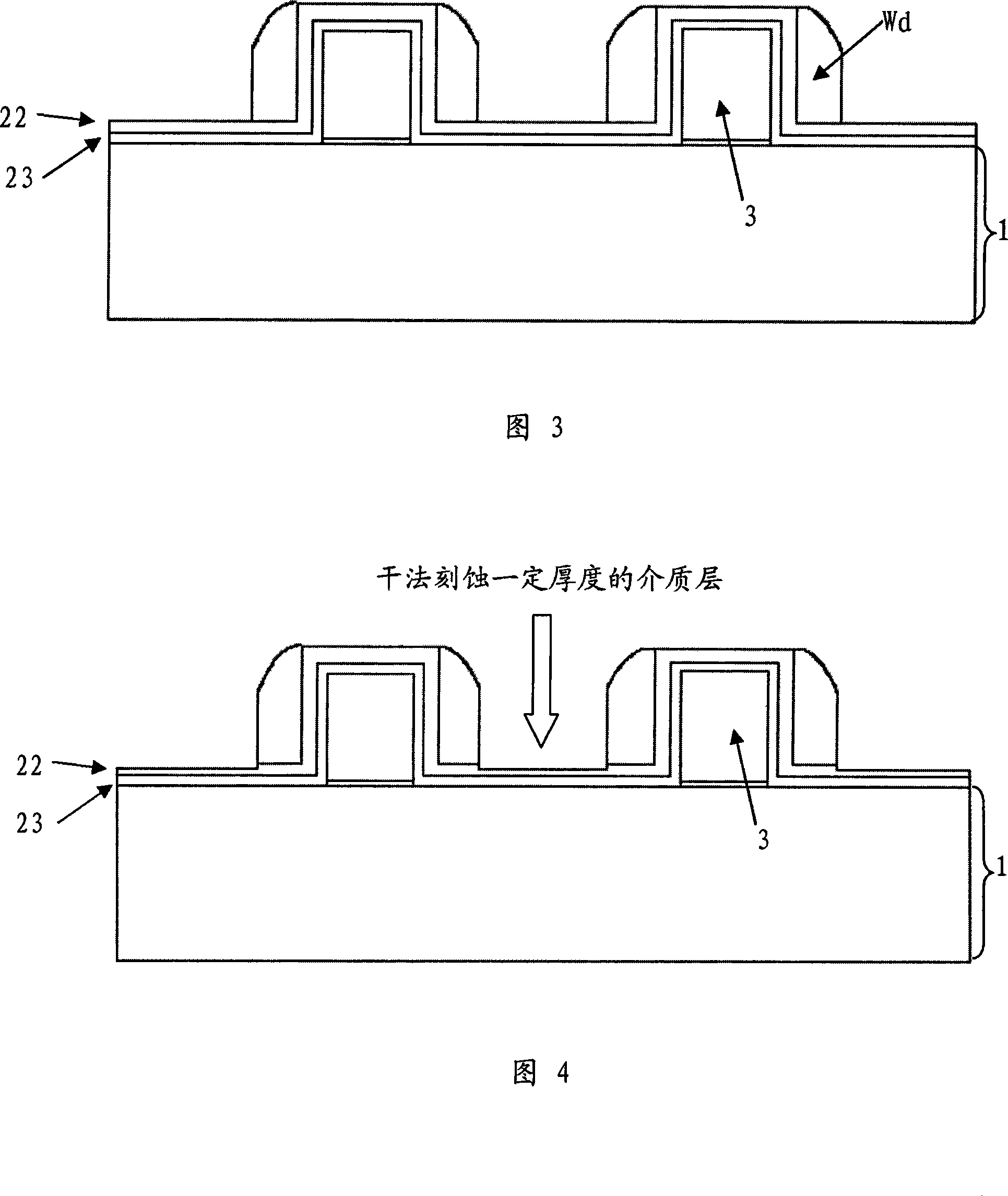
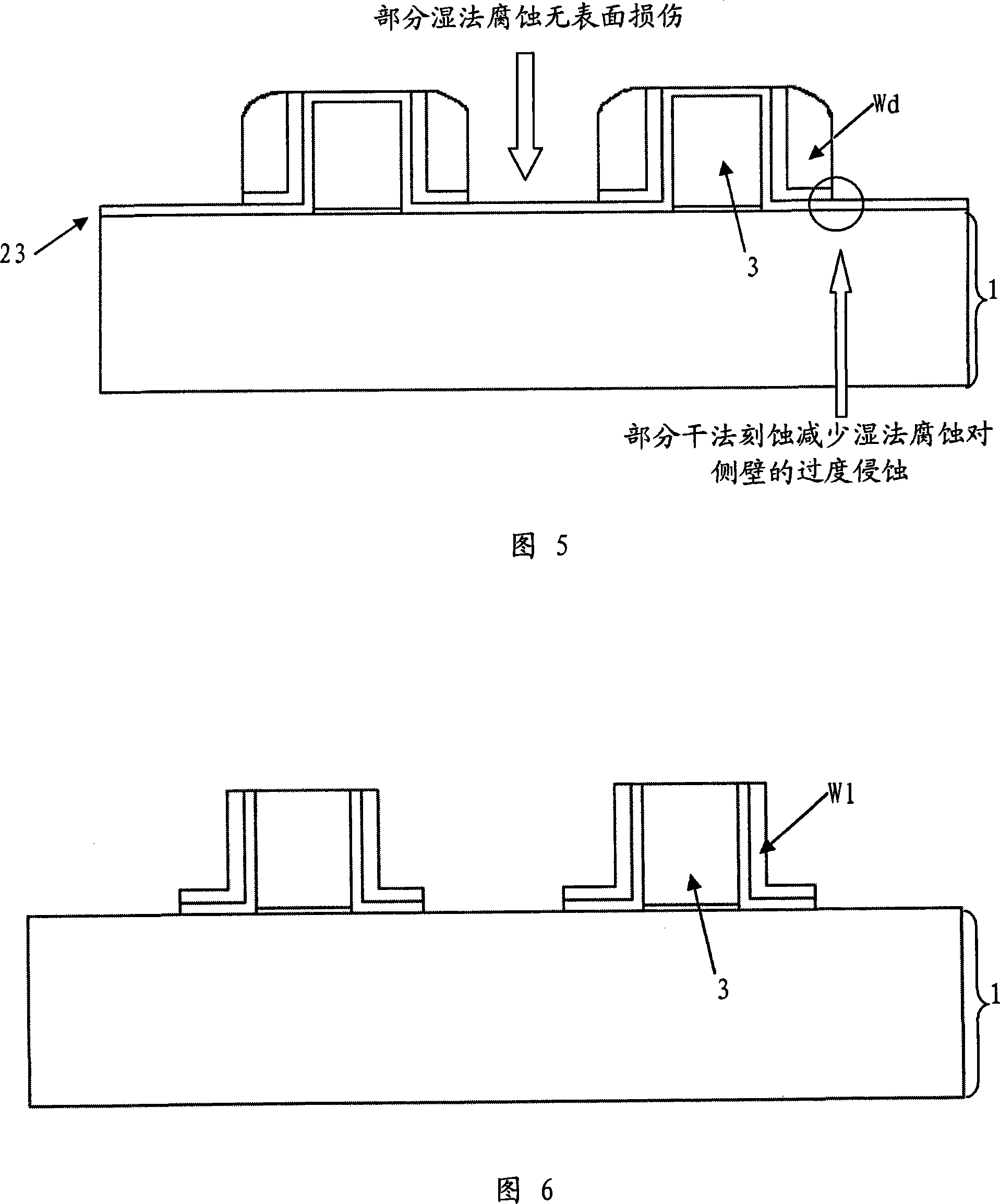
[0021] Please refer to FIG. 2 to FIG. 6 , which are schematic views of the forming process of the L-shaped side wall according to an embodiment of the present invention. First, a composite dielectric layer 2 is deposited on a substrate 1 with a gate 3 structure, wherein the composite dielectric layer 2 includes a sacrificial layer 21 , a dielectric layer 22 and an oxide layer 23 (see FIG. 2 ). In this embodiment, the substrate 1 is, for example, a silicon substrate, the composite dielectric layer 2 is a silicon monoxide / silicon nitride / silicon oxide structure, that is, the sacrificial layer 21 and the oxide layer 23 are silicon oxide layers, and the dielectric layer 22 is silicon nitride layer.
[0022] Next, the sacrificial layer 21 on the si...
PUM
 Abstract
Description
Claims
Application Information