Production method of grids curb wall

A manufacturing method and gate sidewall technology, which is applied in semiconductor/solid-state device manufacturing, electrical components, circuits, etc., can solve the problem of inability to respond to changes in the thickness of sidewall material layers, poor line width and contour consistency of sidewalls, etc. problems, to reduce costs, improve process windows and maintainability, and improve stability

Active Publication Date: 2008-06-11
SEMICON MFG INT (SHANGHAI) CORP +1
View PDF1 Cites 15 Cited by
  • Summary
  • Abstract
  • Description
  • Claims
  • Application Information

AI Technical Summary

Problems solved by technology

[0009] Therefore, the object of the present invention is to provide a method for manufacturing gate sidewalls, to solve the problem that in the existing sidewall manufacturing method, corresponding measures cannot be taken for the thickness variation of the sidewall material layer, so that the line width of the sidewall between different wafers The problem of poor consistency with the outline

Method used


Image

  • Production method of grids curb wall
  • Production method of grids curb wall
  • Production method of grids curb wall

Examples


Embodiment Construction

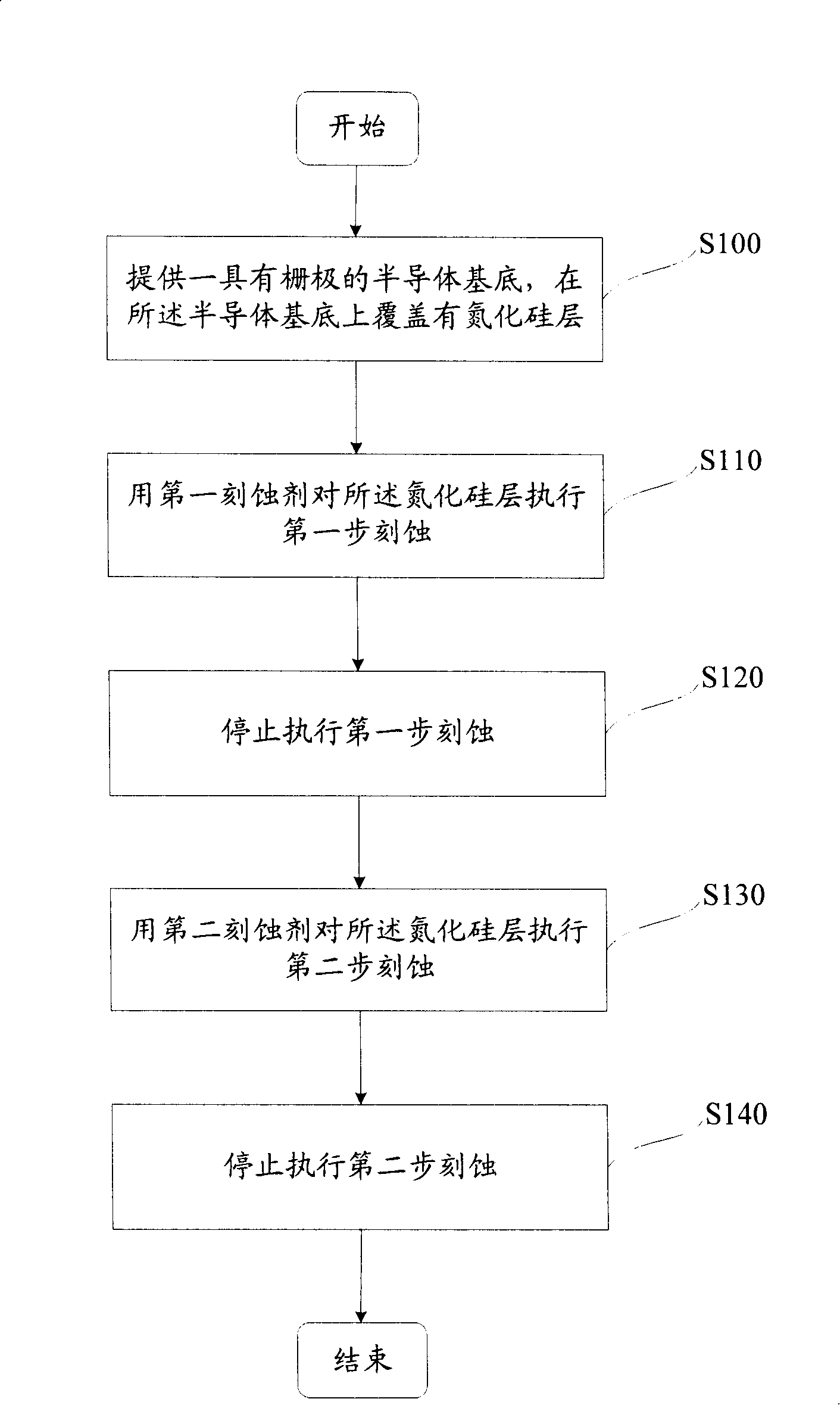
[0031] In order to make the above objects, features and advantages of the present invention more comprehensible, specific implementations of the present invention will be described in detail below in conjunction with the accompanying drawings.

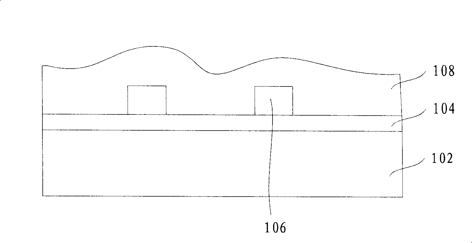
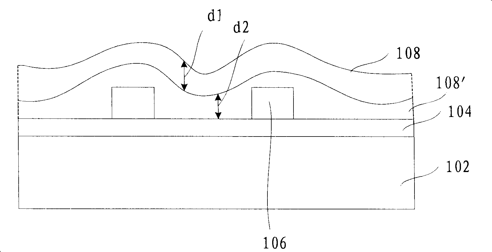
[0032] The manufacturing method of the gate spacer of the present invention first measures the thickness of the dielectric layer deposited on the surface of the gate by an optical critical dimension measurement (OCD, Optical Critical Dimension) method, and then according to the difference between the thickness and the target thickness of the spacer and the calculated The etching rate of the dielectric layer determines the etching time, and the dielectric layer is etched according to the determined time to form sidewalls. The method of the invention can avoid the change of the line width and profile of the side wall after etching caused by the difference in the thickness of the dielectric layer on the wafer, and can improve the consisten...


PUM


Abstract

The invention relates to a manufacturing method for grid side wall, which comprises the following step of: providing a semi-conductor substrate with a grid and forming a dielectric layer on the semi-conductor substrate along the surface of the grid; measuring the thickness of the dielectric layer of the grid side wall and computing the difference between the thickness and the objective thickness of side wall; computing the etching time T according to the difference and the etching rate for the dielectric layer; etching the dielectric layer for the time of T. The method can compensate the variation of thickness of the deposited dielectric layer, thus overcoming the problem of bad uniformity of the carved side wall thickness caused by different thicknesses of the dielectric layer.

Description

technical field [0001] The invention relates to the technical field of semiconductor manufacturing, in particular to a method for manufacturing gate spacers in semiconductor devices. Background technique [0002] The metal oxide semiconductor transistor includes a gate, a source and a drain located in the substrate on both sides of the gate, a conductive channel under the gate, and a gate oxide layer between the conductive channel and the gate . A side wall surrounding the gate is formed on the side wall of the gate. On the one hand, the side wall can protect the gate, and on the other hand, prevent a large dose of source and drain implantation from being too close to the conductive channel so that the source-drain gap may occur. conduction between. Especially with the development of semiconductor manufacturing technology to a higher technology node, the size of the gate is getting smaller and smaller, and the conductive channel in the substrate under the gate is getting s...

Claims


Application Information

Patent Timeline
Patent Type & Authority Applications(China)
IPC IPC(8): H01L21/311H01L21/66H01L21/336
Inventor 杜珊珊张海洋
Owner SEMICON MFG INT (SHANGHAI) CORP
Why Eureka
Try Eureka