

Method for preparing electronic product shell
A technology for electronic products and casings, which is applied in the field of preparation of electronic product casings, can solve problems such as poor decorative effect and inability of casings to transmit light.
- Summary
- Abstract
- Description
- Claims
- Application Information
AI Technical Summary
Problems solved by technology
Method used
Image

Examples
preparation example Construction
[0009] The preparation method of the electronic product casing provided by the present invention includes forming a tin coating on the base material, wherein the method for forming the tin coating on the base material is a DC magnetron sputtering coating method, and the DC magnetron sputtering method includes Next, apply voltage on the magnetron target to sputter and deposit the target substance of the magnetron target on the base material, the target substance is tin, and the sputtering conditions make the thickness of the tin coating not greater than 100 nanometers.
[0010] The sputtering conditions are as long as the thickness of the tin coating is not greater than 100 nanometers. For example, the sputtering conditions include a pressure of 0.1-1.0 Pa, preferably 0.3-0.8 Pa, and a temperature of 20-300 °C, preferably 50-100 °C. °C; the sputtering time is 20-180 seconds, preferably 40-100 seconds. The sputtering conditions make the thickness of the tin coating preferably 20...
Embodiment 1
[0022] This embodiment is used to illustrate the preparation method of the housing of the electronic product provided by the present invention.
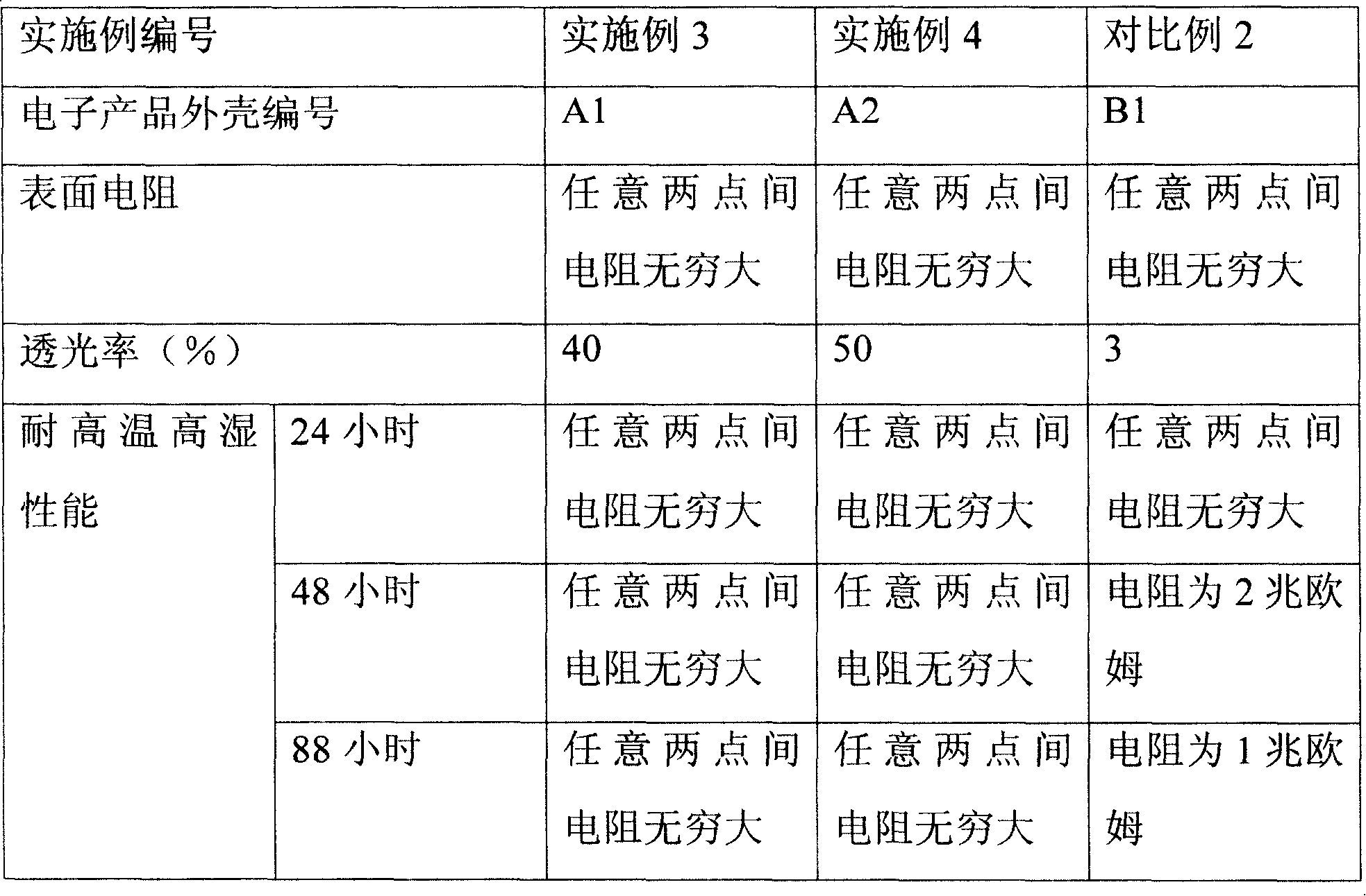
[0023] Using magnetron sputtering equipment (DC magnetron sputtering coating machine, manufactured by Beijing Beiyi Innovation Vacuum Technology Co., Ltd., model JP-900A), the PC sheet with a thickness of 0.8 mm is placed on the magnetron sputtering ion plating On the workpiece rack in the vacuum chamber of the equipment, start the vacuum pump to evacuate, and the vacuum degree in the vacuum chamber reaches 4×10 -3 Pa, fill with argon to make the absolute pressure in the vacuum chamber 0.7 Pa, and adjust the temperature in the vacuum chamber to 70°C. Start the DC power supply (voltage is 450 volts, current is 12 amps) applied on the magnetron target (target material is 99.99% tin), under the above temperature and pressure conditions, sputter for 80 seconds to form on the PC sheet A tin plating layer with a thickness of 60 nanometers...
Embodiment 2
[0025] This embodiment is used to illustrate the preparation method of the housing of the electronic product provided by the present invention.
[0026] Using magnetron sputtering equipment (DC magnetron sputtering coating machine, manufactured by Beijing Beiyi Innovation Vacuum Technology Co., Ltd., model JP-900A), the PET sheet with a thickness of 1 mm is placed on the magnetron sputtering equipment. On the workpiece rack in the vacuum chamber, start the vacuum pump to evacuate, and the vacuum degree in the vacuum chamber reaches 6×10 -3 Pa, fill with argon to make the absolute pressure in the vacuum chamber 0.5 Pa, and adjust the temperature in the vacuum chamber to 60°C. Start the DC power supply (voltage is 420 volts, current is 10 amps) that is applied on the magnetron target (the target material is 99.99% tin), and under the above-mentioned temperature and pressure conditions, sputter 60 seconds, form on the PC sheet material A tin plating layer with a thickness of 45 ...
PUM
| Property | Measurement | Unit |
|---|---|---|
| Thickness | aaaaa | aaaaa |
| Thickness | aaaaa | aaaaa |
| Thickness | aaaaa | aaaaa |
Abstract
Description
Claims
Application Information