System and method for testing NVM chip

A chip testing and chip technology, applied in electronic circuit testing, electrical measurement, measuring devices, etc., can solve the problems of inability to test chips at the same time, waste of testing resources, affecting the efficiency of testing, etc., so as to shorten the testing time and speed up the output. , the effect of expanding the ability of co-testing

Inactive Publication Date: 2008-06-18
SHANGHAI HUA HONG NEC ELECTRONICS
View PDF0 Cites 12 Cited by
  • Summary
  • Abstract
  • Description
  • Claims
  • Application Information

AI Technical Summary

Problems solved by technology

[0006] The existing NVM chip test system and method cannot test more chips at the same time, which will not only affect the efficiency of the test, but also cause a great waste of test resources

Method used


Image

  • System and method for testing NVM chip
  • System and method for testing NVM chip
  • System and method for testing NVM chip

Examples


Embodiment Construction

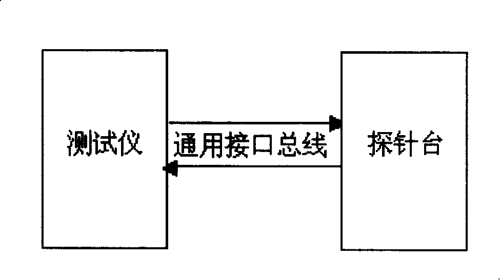
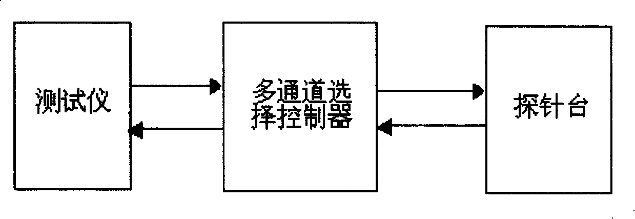
[0017] Such as image 3 As shown, the NVM chip test system of the present invention includes a tester that is connected in sequence and performs signal transmission, a multi-channel selection controller that selects test channels, and a probe station. The tester is connected to the probe station through a multi-channel selection controller that selects the test channel to test the chip. And the multi-channel selection controller of the gating test channel is composed of multiple relays. Such as Figure 4 As shown, before the test channel of the tester is connected to the probe of the probe station, a multi-channel selection controller composed of relays is used, and the multi-channel selection controller selects the test channel during testing.

[0018] Such as Figure 5 As shown, the NVM chip testing method of the present invention includes the following steps: using the NVM chip testing system of the present invention, before the test channel is connected to the probe of the prob...


PUM


Abstract

The invention discloses an NVM chip test system, comprising a test instrument, a multi-channel selection controller used for selecting test channels and a probe station which are sequentially connected for signal transmission. The invention also discloses an NVM chip test method including the following steps: selecting test channels; connecting the test channels and the probe; modifying files used for automatically distributing test sources to realize the automatic communication between the test instrument and the probe station; implementing a first flow of chip test to judge whether the chip is normal or not; determining the channel required to be cut according to the normal or abnormal states of the chip; closing the channels on the multi-channel selector sequentially; selecting and going-through a special objective chip to write the test results into the chip; generating and storing classified information of the chip test results; reading classified information of the chip test results and confirming the test results; implementing a second test flow to judge whether the chip is normal or not. The invention can make use of the test channels to a max extent so as to enhance a common test quantity and to shorten test time to raise a manufacturing speed of the product.

Description

Technical field [0001] The present invention relates to the field of integrated circuit testing, in particular to a non-volatile memory (NVM) chip testing system in the field of integrated circuit testing, and a NVM chip testing system using the NVM chip testing system is also designed method. Background technique [0002] In some test systems, the number of channels can use a lot of test resources, about 1300 channels. But existing test systems such as figure 1 As shown, including the tester, probe station, universal interface bus, and communication software, only 32 simultaneous tests are supported. Because the test system hardware does not support, and the software including the probe station does not support more chips to be tested at the same time, when testing some chips with small pin numbers, such as 5 Pad chips, only 32×5=160 channels are used. The remaining 1140 channels are not used at all and are in an idle state, wasting test resources. [0003] At present, due to h...

Claims


Application Information

Patent Timeline
Patent Type & Authority Applications(China)
IPC IPC(8): G11C29/56G01R31/28G01R31/00
Inventor 陈凯华谢晋春陈婷桑浚之辛吉升
Owner SHANGHAI HUA HONG NEC ELECTRONICS
Why Eureka
Try Eureka