

Magnetic storage element and memory
A storage element and storage layer technology, applied in the direction of static memory, digital memory information, electrical components, etc., to achieve the effect of reducing current flow, low power consumption, and reducing power consumption
- Summary
- Abstract
- Description
- Claims
- Application Information
AI Technical Summary
Problems solved by technology
Method used
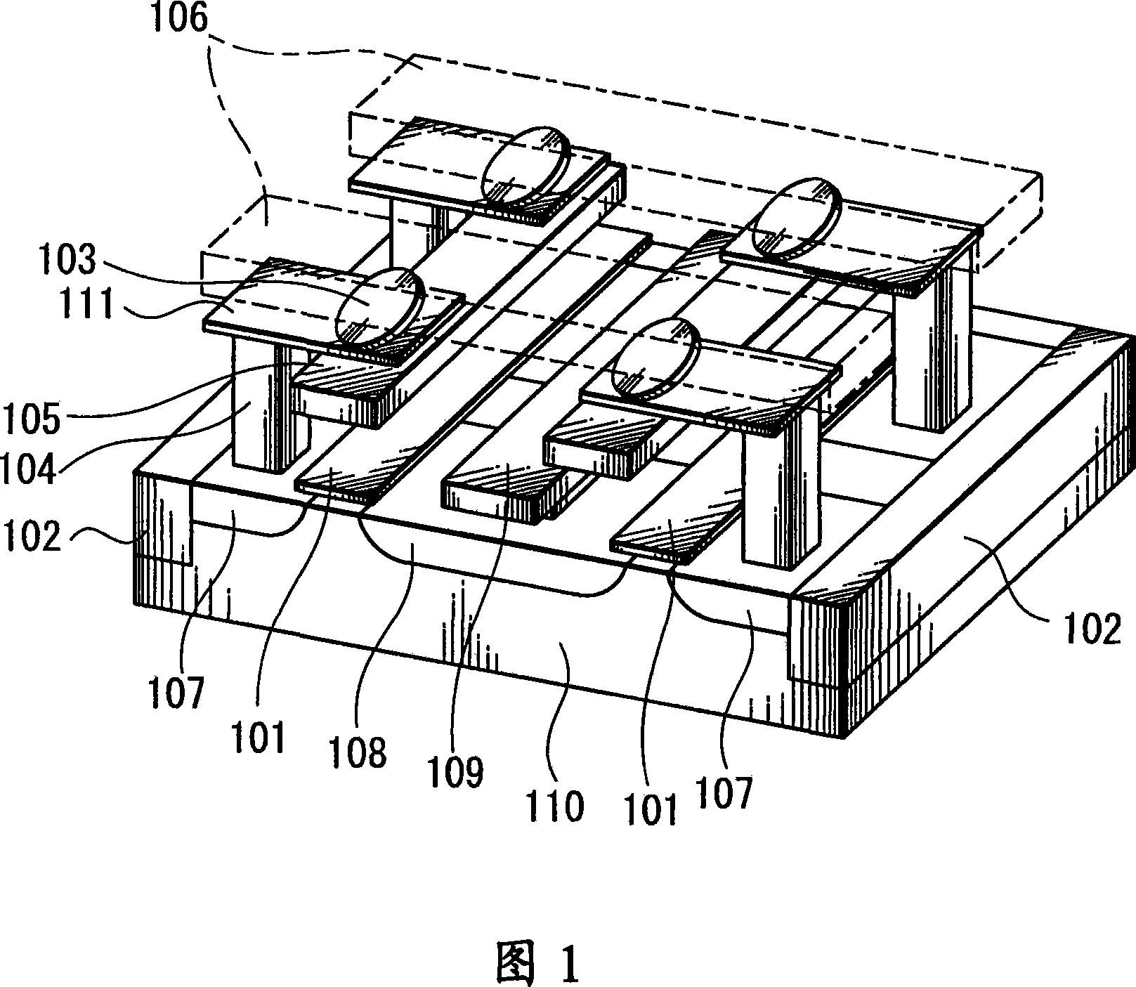
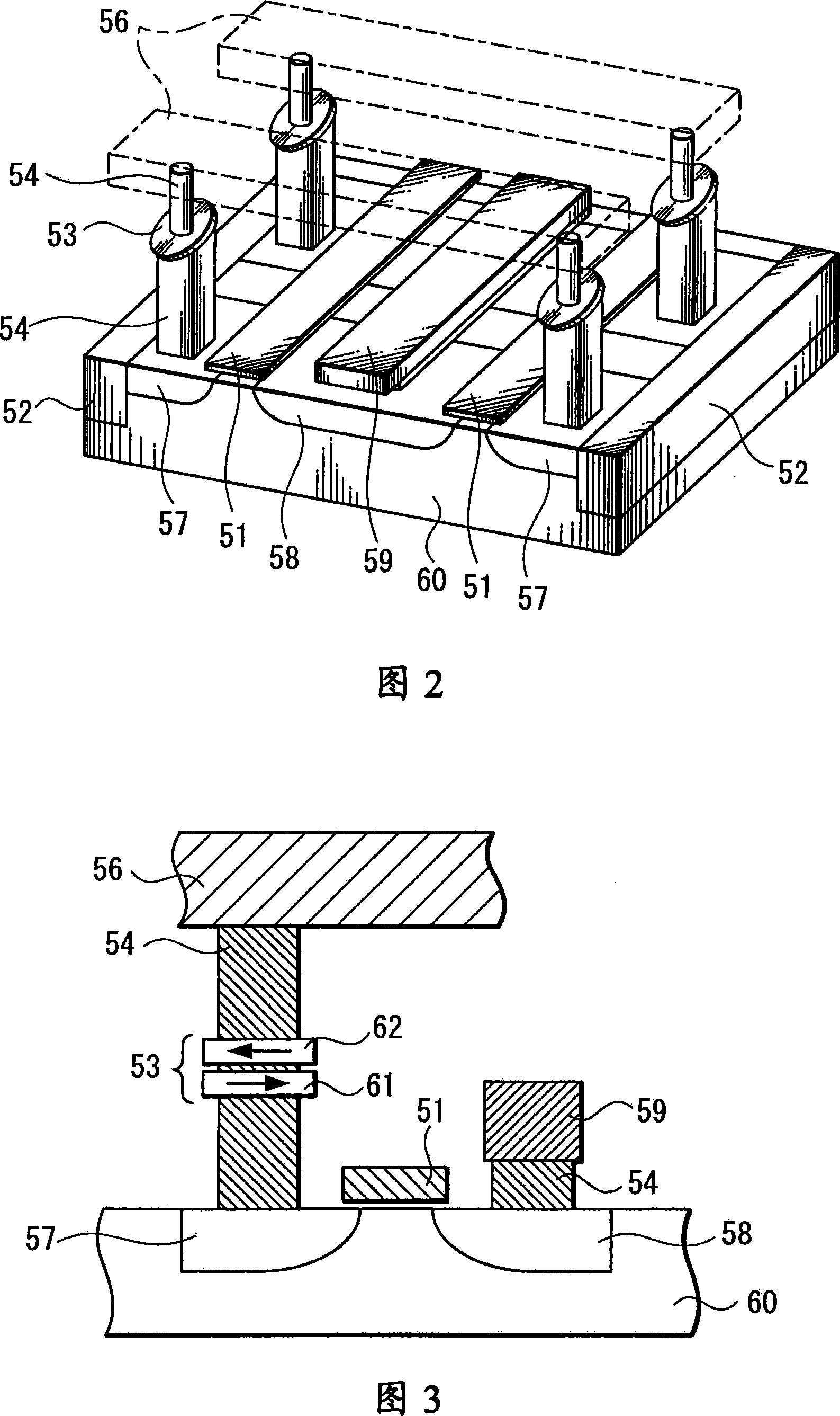
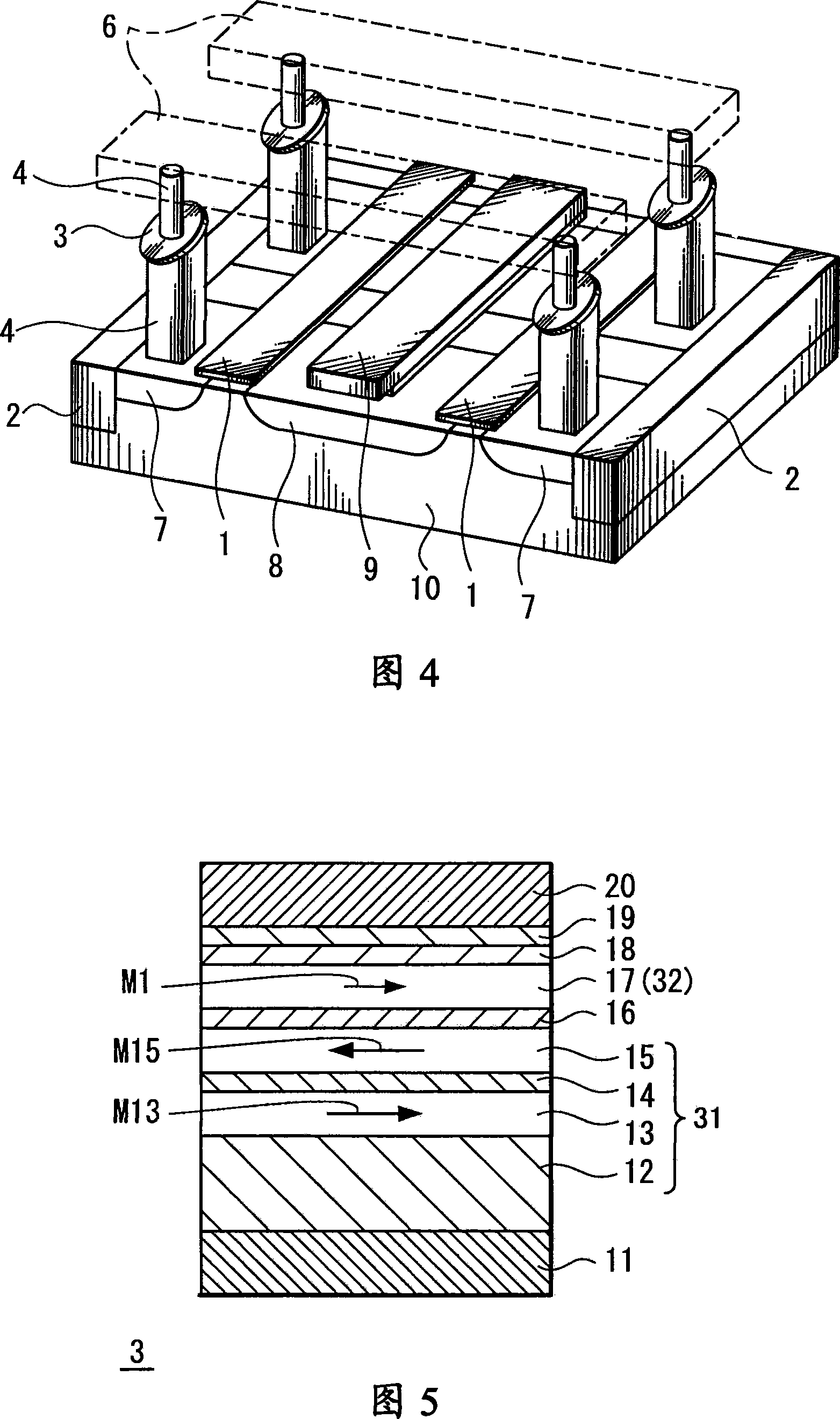
Image

Examples
example
[0198] A thermally oxidized film having a thickness of 2 µm was formed on a silicon substrate having a thickness of 0.575 mm, and the memory element 3 having the configuration shown in FIG. 5 was formed on top of the silicon substrate.
[0199] Specifically, the material and film thickness configured as the memory element 3 shown in FIG. 5 are selected for each layer as follows. A Ta film with a thickness of 3 nm was selected as the bottom layer 11 . PtMn with a thickness of 30 nm is selected as the antiferromagnetic layer 12 . A CoFe film with a thickness of 2.2 nm was selected as the ferromagnetic layer 13 . A CoFeB film having a thickness of 2 nm is selected as the ferromagnetic layer 15 of the magnetization fixed layer 31 . A Ru film having a thickness of 0.8 nm was selected as the nonmagnetic layer 14 of the magnetization fixed layer 31 having a laminated ferromagnetic structure. A MgO film with a thickness of 0.8 nm was selected as the tunnel insulating layer 16 . A ...
PUM
| Property | Measurement | Unit |
|---|---|---|
| area | aaaaa | aaaaa |
| thickness | aaaaa | aaaaa |
| thickness | aaaaa | aaaaa |
Abstract
Description
Claims
Application Information