Method for fabricating CMOS image sensor

A technology of an image sensor and a manufacturing method, which is applied in the manufacturing of semiconductor/solid-state devices, electric solid-state devices, semiconductor devices, etc., can solve problems such as difficulty in achieving concentration distribution, limitation of boron (B) diffusion, etc.

Inactive Publication Date: 2008-07-02
DONGBU HITEK CO LTD
View PDF0 Cites 7 Cited by
  • Summary
  • Abstract
  • Description
  • Claims
  • Application Information

AI Technical Summary

Problems solved by technology

[0028] However, in conventional techniques, there are limitations in controlling the diffusion of boron (B) with small mass and fast diffusion
Therefore, ion implantation performed at low energies is difficult to achieve the desired form of concentration distribution

Method used


Image

  • Method for fabricating CMOS image sensor
  • Method for fabricating CMOS image sensor
  • Method for fabricating CMOS image sensor

Examples


Embodiment Construction

[0037] Hereinafter, exemplary embodiments according to the present invention will be described in detail with reference to the accompanying drawings.

[0038] Reference Figure 2A to Figure 2E , Showing a cross-sectional view of a method of manufacturing a CMOS image sensor according to the present invention.

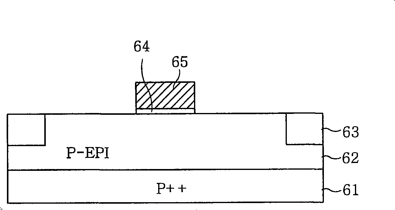
[0039] Such as Figure 2A As shown, an epitaxial process is used to form a low concentration of P on the semiconductor substrate 101 - Type epitaxial layer 102, in which the semiconductor substrate 101 is, for example, a high-concentration P ++ Type single crystal silicon.

[0040] The epitaxial layer 102 is formed to have a large and deep depletion region in the photodiode, thereby enhancing the ability of the low-voltage photodiode to collect light charges and also improving its light sensitivity.

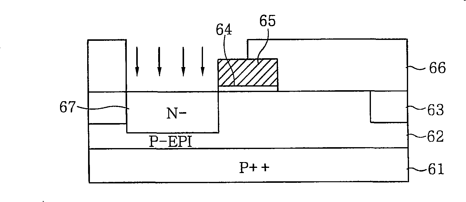
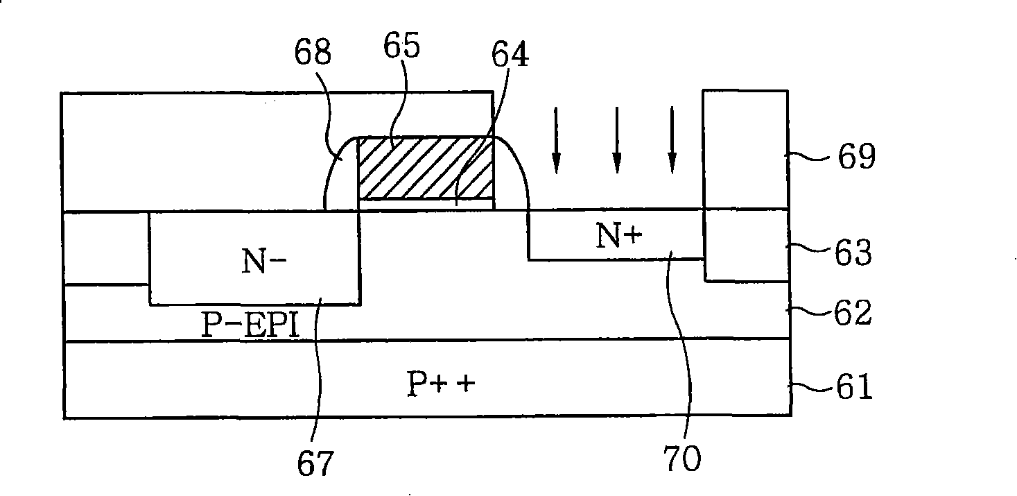
[0041] After that, the active region and the device isolation region are defined in the semiconductor substrate 101. Then, a device isolation film 103 is formed in the device ...


PUM


Abstract

A method for fabricating a Complementary Metal Oxide Semiconductor (CMOS) image sensor includes implanting first conductive type dopants into a semiconductor substrate and forming a photodiode region in a surface of the semiconductor substrate, performing spike annealing to the semiconductor substrate having the photodiode region formed thereon, to thereby suppress diffusion of the first conductive type dopants and remove an interstitial between lattices, and implanting second conductive type dopants into an upper part of the photo diode region to form a second conductive type diffusion region.

Description

Technical field [0001] The present invention relates to a method for manufacturing an image sensor, in particular to a method for manufacturing a CMOS image sensor, which is used to improve the characteristics of the image sensor. Background technique [0002] Generally, an image sensor is a semiconductor device that converts an optical image into an electrical signal. Image sensors can be mainly divided into charge coupled devices (CCD) and CMOS image sensors (CIS). [0003] The CCD has a plurality of photodiodes (PD) arranged in a matrix, and these photodiodes convert optical signals into electrical signals. The CCD includes multiple vertical charge coupled devices (VCCD), horizontal charge coupled devices (HCCD), and readout amplifiers. The VCCD is formed between the respective photodiodes arranged in a matrix, and transfers the charge generated by each photodiode in the vertical direction. The HCCD transfers the charge transferred by each VCCD in the horizontal direction. The...

Claims


Application Information

Patent Timeline
Patent Type & Authority Applications(China)
IPC IPC(8): H01L21/822H01L31/18H01L21/322
CPCH01L27/14603H01L27/14689
Inventor 李政皓
Owner DONGBU HITEK CO LTD
Why Eureka
Try Eureka