CMOS image sensor and its manufacture method

A pattern and device technology, applied in CMOS image sensors and their manufacturing, in the field of increasing the capacitance of the floating diffusion area, can solve the problems of easy noise generation and low capacitance, etc.

Inactive Publication Date: 2008-07-02
DONGBU HITEK CO LTD
View PDF0 Cites 13 Cited by
  • Summary
  • Abstract
  • Description
  • Claims
  • Application Information

AI Technical Summary

Problems solved by technology

Noise can easily become a problem if low capacitance occurs

Method used


Image

  • CMOS image sensor and its manufacture method
  • CMOS image sensor and its manufacture method
  • CMOS image sensor and its manufacture method

Examples


Embodiment Construction

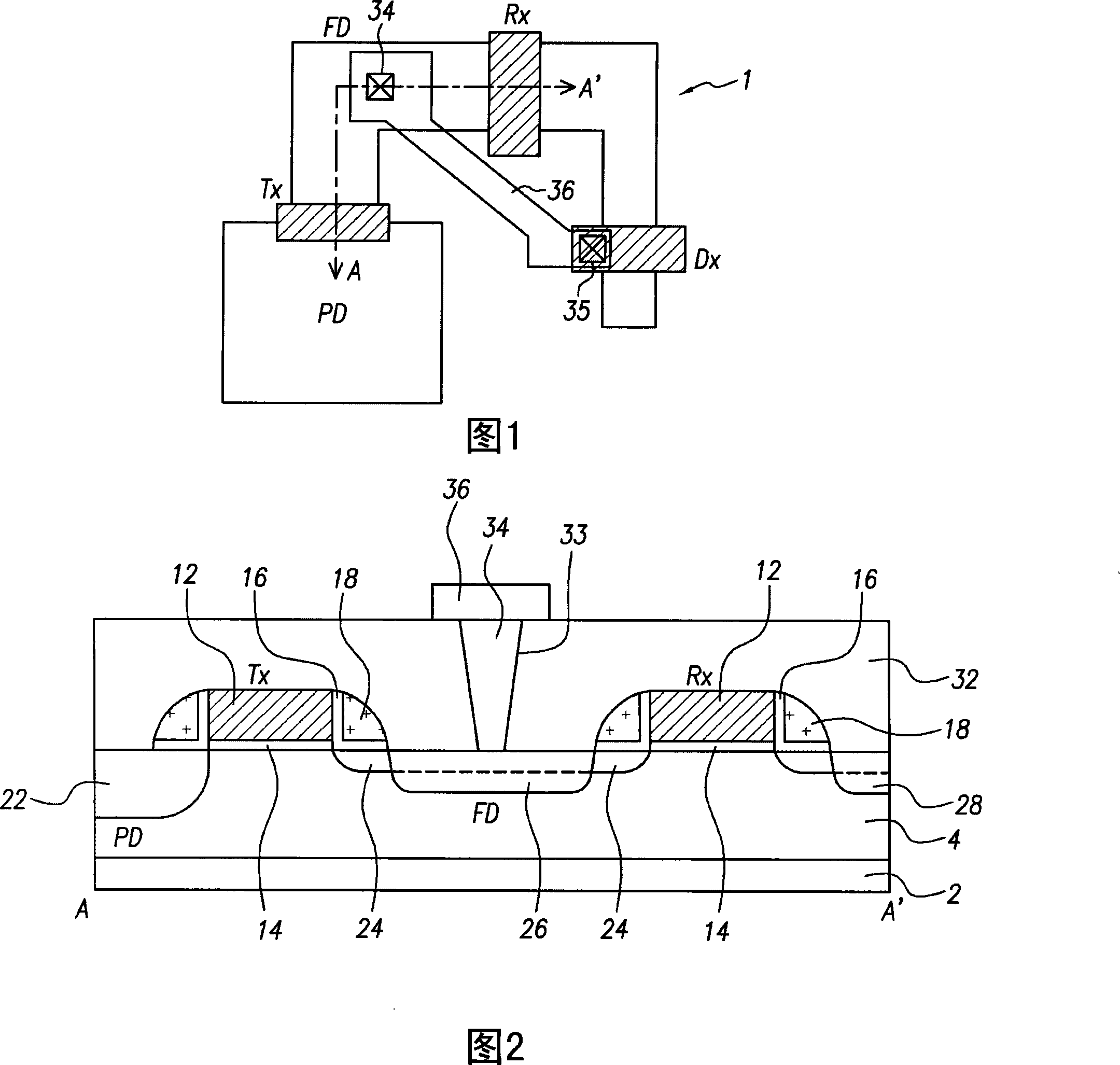
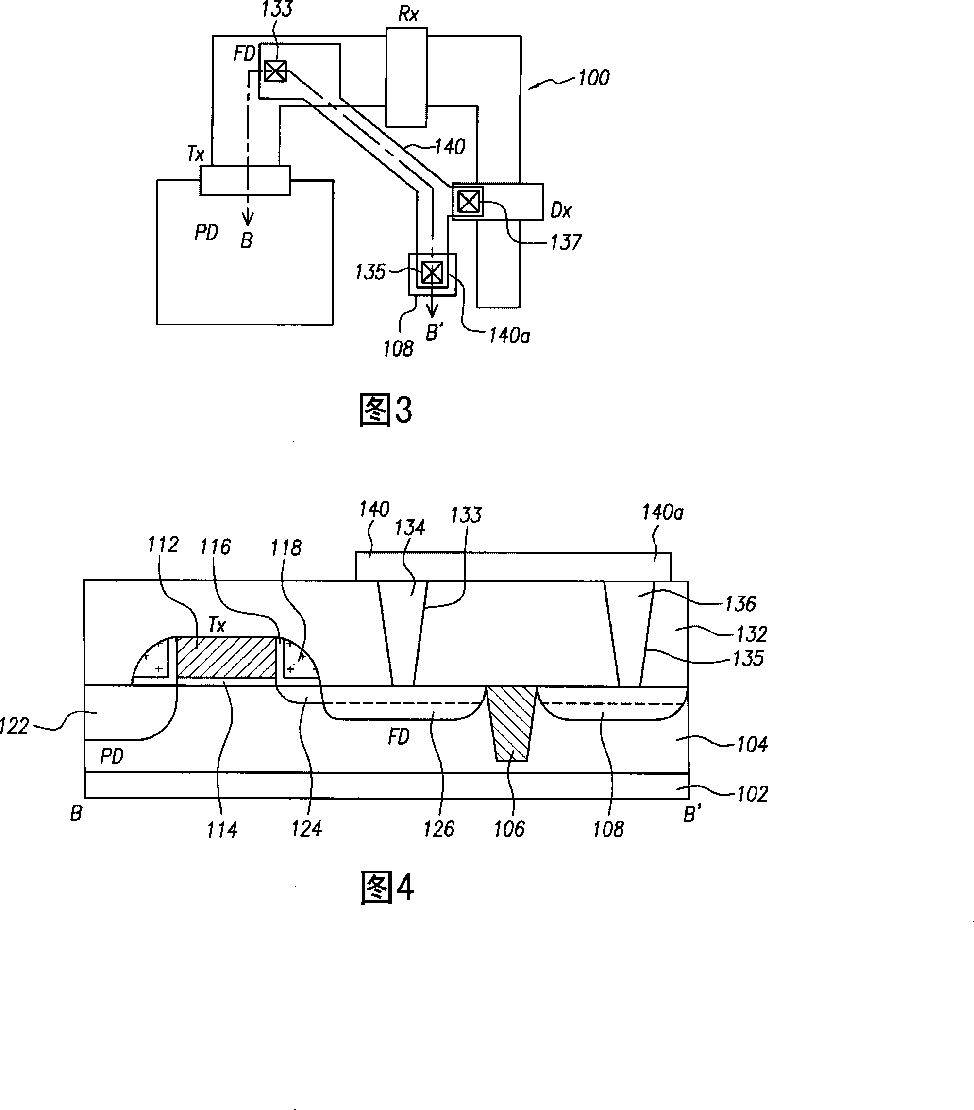
[0038] As shown in the example of FIG. 3, the CMOS image sensor according to the embodiment of the present invention may include a photodiode region PD formed in the widest part of the active region 100. An island-type active region (also referred to as an "island region") 108 may be formed adjacent to the photodiode region PD. The junction capacitance of the active region 108 may be formed to be parallel to the source region 126. The transfer transistor Tx, the reset transistor Rx, and the drive transistor Dx may overlap the active region 100 except for the photodiode region PD. In addition to being adjacent to the photodiode region PD, the island region 108 may also be formed in other positions. In addition, the island area 108 may also include at least one or more island areas 108.

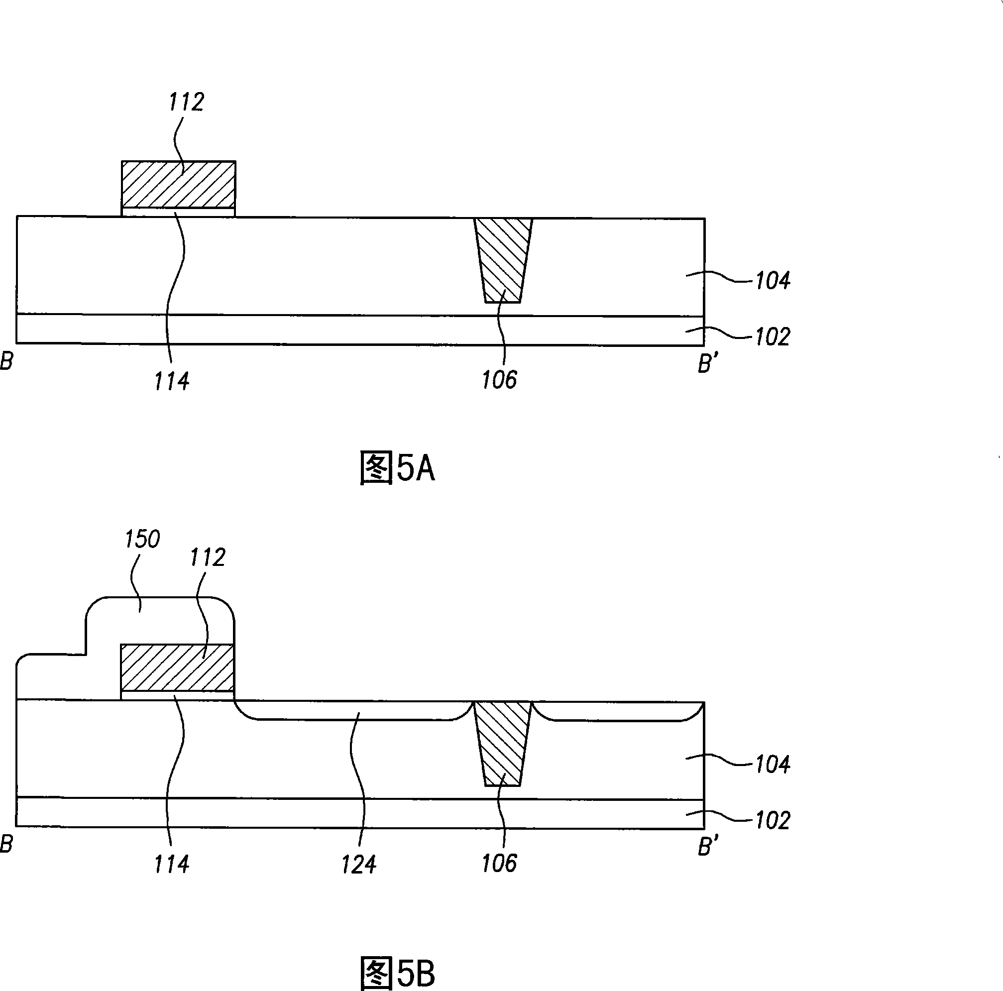
[0039] As shown in the example of FIG. 4, the CMOS image sensor according to the embodiment of the present invention may further include a p++ type semiconductor substrate 102, a p epitaxial layer ...


PUM


Abstract

A CMOS image sensor and a manufacturing method thereof, the CMOS image sensor comprising: an epitaxial layer formed above a semiconductor substrate; a gate electrode formed above the epitaxial layer; a gate metal formed above a floating diffusion region of the epitaxial layer; The n+ type source region and the drain region are formed in the epitaxial layer; the gate spacer is formed on both side walls of the gate electrode and the gate metal; the insulating interlayer is formed on the gate electrode, the gate spacer and the gate metal Above the epitaxial layer of the layer, the insulating interlayer includes: a first contact hole passing through the insulating interlayer and exposing the source region; a second contact hole passing through the insulating interlayer and exposing the gate metal; a first contact plug formed in the first contact hole and connected to the source region; a second contact plug formed in the second contact hole and connected to the gate metal; and a metal line formed over the first contact plug and the second contact plug to electrically connect the source region to the gate extremely metallic. The present invention can increase the capacitance of the floating diffusion (FD).

Description

[0001] This application claims the priority of Korean Patent Application No. 10-2006-0137357 filed on December 29, 2006, and the entire content of the patent application is incorporated herein by reference. Technical field [0002] The invention relates to a CMOS image sensor, in particular to a CMOS image sensor and a manufacturing method thereof. Although the present invention has a wide range of applications, it is particularly suitable for increasing the capacitance of the floating diffusion (FD). Background technique [0003] The image sensor is a device that converts optical images into electrical signals. Image sensors are generally classified into complementary metal oxide semiconductor (CMOS) image sensors and charge coupled device (CCD) image sensors. [0004] Compared with CMOS image sensors, CCD image sensors show better sensitivity and lower noise, but it is difficult to achieve high integration and low power consumption. On the contrary, the manufacturing process of ...

Claims


Application Information

Patent Timeline
Patent Type & Authority Applications(China)
IPC IPC(8): H01L27/146H01L23/522H01L21/822H01L21/768
CPCH01L27/14603H01L27/14609H01L27/14643H01L27/14689H01L29/66659H01L29/7833H01L29/7835H01L27/146
Inventor 任劲赫
Owner DONGBU HITEK CO LTD
Why Eureka
Try Eureka