Big width laser marking solar cell

A solar cell and laser marking technology, which is applied to circuits, electrical components, sustainable manufacturing/processing, etc., can solve problems such as marking large-format thin-film batteries, and achieve improved photoelectric conversion efficiency, fast marking speed, The effect of increasing the effective area

Active Publication Date: 2008-07-02
李毅
View PDF3 Cites 13 Cited by
  • Summary
  • Abstract
  • Description
  • Claims
  • Application Information

AI Technical Summary

Problems solved by technology

At present, since the manufactured thin-film batteries are getting bigger and bigger, and the previous laser-marked thin-film battery products are basically simple graphics composed of straight lines, the marking of large-format thin-film batteries and special graphics cannot be solved with the existing technology.

Method used


Image

  • Big width laser marking solar cell
  • Big width laser marking solar cell
  • Big width laser marking solar cell

Examples


example 2

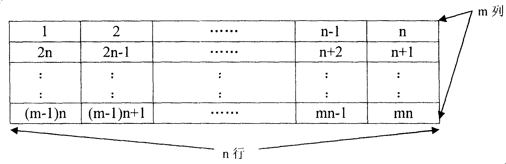
[0036] Example 2, embodiment figure, see figure 1 and Figure 7 Same as above, m=4, n=2, produce amorphous silicon thin-film solar panels with unit cell spacing of 10mm and external dimensions of 1000mm×2000mm×3.0mm.

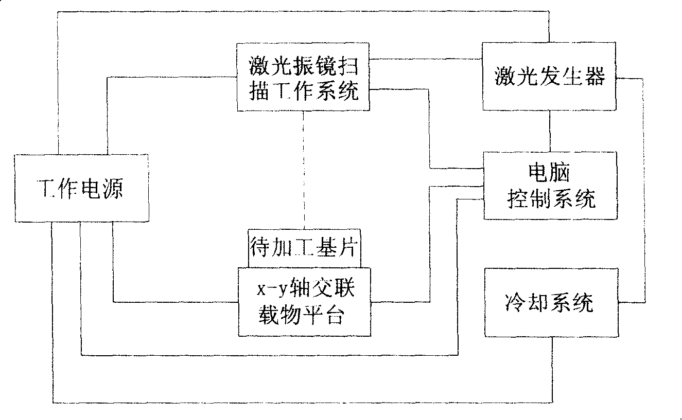
[0037] Front electrode graphic production: place the composite transparent conductive film glass film with a size of 1000mm×2000mm×3.0mm facing up, place it on the X-Y axis loading work platform, start the large-format infrared laser marking system, and import the front electrode of the battery. engrave graphics, and set the marking range of the laser galvanometer scanning system to 500mm×500mm, divide the 1000mm×2000mm×3.0mm substrate to be marked into 8 marking areas of 500mm×500mm, and adopt multi-format marking In the way of engraving, 100 insulating isolation lines parallel to the long side with a spacing of 10mm are marked on the continuous conductive film of the substrate, see Figure 7 The part shown in 1'. In this way, the continuous conductive film ...


PUM


Abstract

The invention discloses a scan system of a large document laser vibrating mirror used for marking and carving a solar energy battery by the laser, belonging to a technical field of manufacture of the solar energy battery with an amorphous silicon film. The invention aims at improving the marking and carving speed and precision of the solar energy battery products with the amorphous silicon films. The invention is technically characterized by computer program control, the laser vibrating mirror scanning system with the document of 400mm-600mm, marking and carving as well as positioning coordinate points by the laser and adopting the production method of multi-document or single document to produce the solar energy battery with the amorphous silicon film. The invention is also technically characterized in that when the laser vibrating mirror scanning system is started, a X-Y cross-linking platform is in a halted state. Unidirectional displacement of an X or a Y axoneme bar is promoted for m or n equal divisions to mark and carve the area. The invention has the effects that the maximum linear velocity of marking and carving the high-speed solar energy battery with the amorphous silicon film with the large document is 400m/min and complex graphs can be marked and carved. The invention has the advantages of not influencing the precision of a minimal marking-carving path by the weight of a mechanical platform and operation speed as well as high production efficiency and low cost.

Description

technical field [0001] The invention relates to the application of a large-format laser marking system in the manufacture of amorphous silicon thin-film solar cells, and specifically belongs to the technical field of manufacturing amorphous silicon thin-film solar cells. Background technique [0002] At present, laser marking technology has been widely used in the production of amorphous silicon thin film solar cells. The processing technology adopted by the laser marking system can be roughly divided into the following types: one is to fix the laser output marking head, and the The amorphous silicon solar cell (hereinafter referred to as the substrate) is placed on the X-Y cross-connecting screw system loading work platform, and the graphic marking on the substrate is completed through the movement of the X-Y cross-connecting screw system. The second type is to fix the laser output marking head on the X screw rod of the separate X-Y screw rod system, and fix the loading wor...

Claims


Application Information

Patent Timeline
Patent Type & Authority Applications(China)
IPC IPC(8): H01L31/18H01L31/20
CPCY02P70/50
Inventor 李毅李全相
Owner 李毅
Why Eureka
Try Eureka