Device for correcting illumination homogeneity

A technology for uniformity correction and illumination field, which is applied in photolithography process exposure devices, microlithography exposure equipment, etc. It can solve problems such as increasing the complexity of the correction system, and achieve the effect of avoiding light leakage and shadows and controlling uniformity.

Active Publication Date: 2008-07-16
SHANGHAI MICRO ELECTRONICS EQUIP (GRP) CO LTD
View PDF2 Cites 20 Cited by
  • Summary
  • Abstract
  • Description
  • Claims
  • Application Information

AI Technical Summary

Problems solved by technology

Although the above-mentioned light leakage and shadow effects can be eliminated by using this kind of compensation plate with transmittance distribution, it is necessary to add an additional compensation plate, and the transmittance distribution of the compensation plate needs to correspond to all the gaps of the correction element, which will inevitably increase the correction system. the complexity

Method used


Image

  • Device for correcting illumination homogeneity
  • Device for correcting illumination homogeneity
  • Device for correcting illumination homogeneity

Examples


Embodiment approach

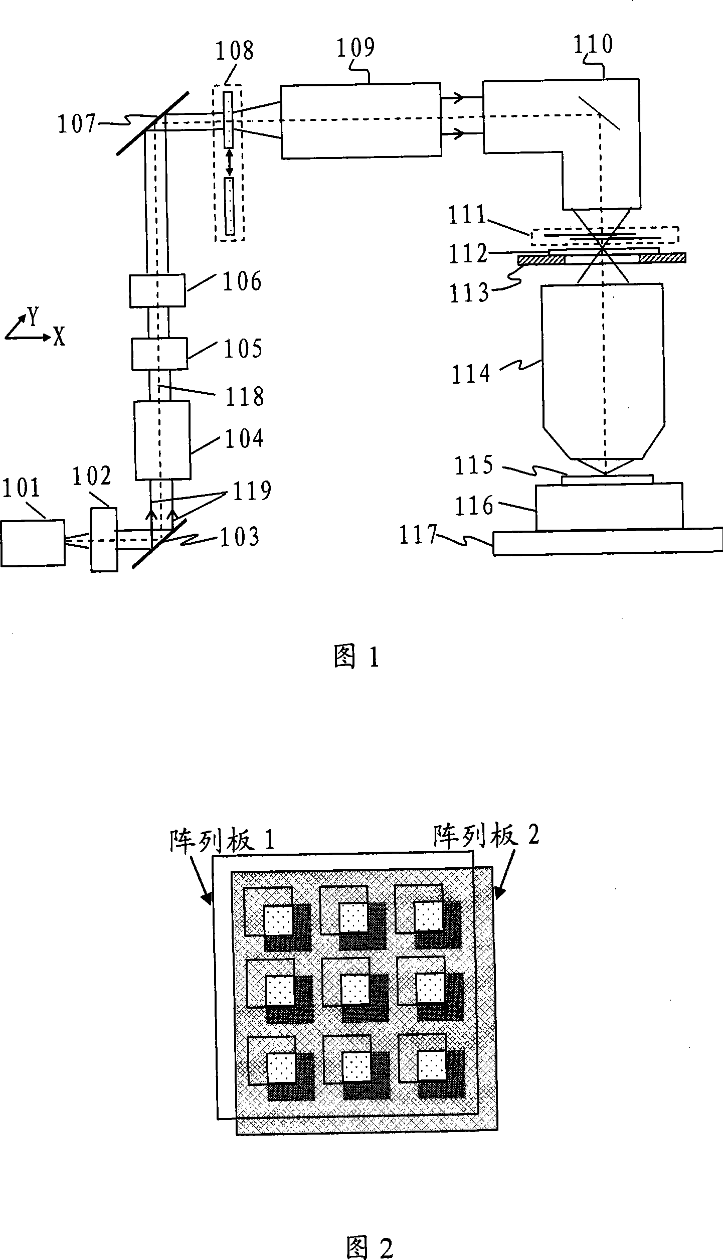
[0034] As shown in FIG. 1 , it is a schematic structural diagram of an exposure projection system applied to the uniformity correction device of the present invention. Wherein, the light source 101 generates a laser beam for exposure, which may be a laser light source of 248nm, or 193nm, or other wavelengths. The beam 119 emitted by the light source is first collimated by the beam expander 102, and the elliptical light is converted into a circular beam; the reflector unit 103 can be a single reflector, or a complex transmission system comprising multiple reflectors, which The laser beam 119 emitted from the beam expander 102 is transmitted to the beam positioning unit 104; the beam positioning unit 104 can correct the incident position and angle of the beam 119 by sampling and analyzing the beam; then the beam 119 passes through the energy used to control the lighting system The adjustable optical attenuator 105 and the energy monitoring unit 106; after passing through the ref...


PUM


Abstract

The invention provides a lighting evenness correcting device arranged near a mask plate or near the optical conjugate planes of the mask plate. The device comprises a plurality of correcting component pairs arranged on the cross section of an illuminating beam, wherein the correcting component pairs are arranged at intervals in a non-scan direction and are overlapped in scanning direction; moreover, the correcting component pairs comprises a first correcting component inserted into a rectangular illumination field in scanning direction and a second correcting component inserted into the rectangular illumination field in a direction opposite to the scanning direction; the first correcting component and the second correcting component are in the shape of parallel flat plates on the section of the scanning direction and light beam transmission direction, and can respectively complete at least one dimensional motion in the scanning direction; both correcting components are provided with opposite transmittance distribution changing with position. The invention can prevent light leakage and shadow caused by the gap formed between adjacent correcting components; meanwhile, the invention can control the distribution of integral energy in the scanning direction and the evenness of the entire illumination field.

Description

technical field [0001] The invention relates to an illumination uniformity correction device applied in a photolithography system. Background technique [0002] Photolithography is an important process in semiconductor manufacturing, which precisely transfers the pattern on the mask to the substrate (such as: silicon wafer). In a lithography system, an illumination system is included between the laser source and the mask to generate the desired illumination pattern and illumination field distribution. In lithography, it is required that the illumination field generated by the illumination system is as uniform as possible, and the uniformity error is as small as possible, so that the entire illumination beam can be evenly irradiated on the mask and evenly projected onto the substrate. Illumination uniformity affects linewidth uniformity across the exposure field. [0003] A step-and-scan lithography system is a typical lithography system, which has a rectangular illuminatio...

Claims


Application Information

Patent Timeline
Patent Type & Authority Applications(China)
IPC IPC(8): G03F7/20
Inventor 程波涛李仲禹
Owner SHANGHAI MICRO ELECTRONICS EQUIP (GRP) CO LTD
Why Eureka
Try Eureka