

LED and its making method
A technology of light-emitting diodes and manufacturing methods, which is applied to electrical components, circuits, semiconductor devices, etc., and can solve problems such as performance degradation of light-emitting elements, increase in density, and shortened life of light-emitting elements
- Summary
- Abstract
- Description
- Claims
- Application Information
AI Technical Summary
Problems solved by technology
Method used
Image

Examples
Embodiment Construction
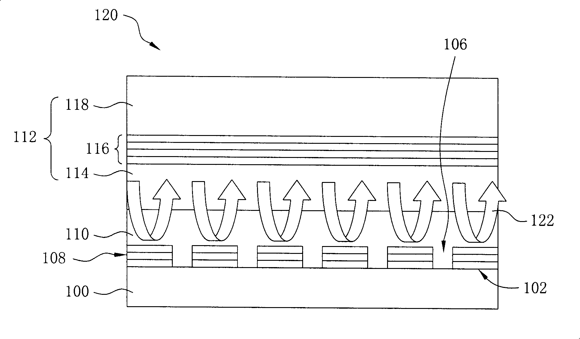
[0021] The invention discloses a light-emitting diode and a manufacturing method thereof. Periodic reflective structures are provided between the substrate and the epitaxial structure, and the high-quality epitaxial structure can improve the light extraction rate of the light-emitting diode element and effectively Extend the life of the components, but also improve the operating quality of the components. In order to make the narration of the present invention more detailed and complete, refer to the following description and cooperate Figure 1 to Figure 8 icon of the .
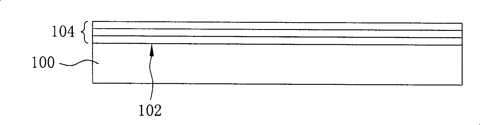
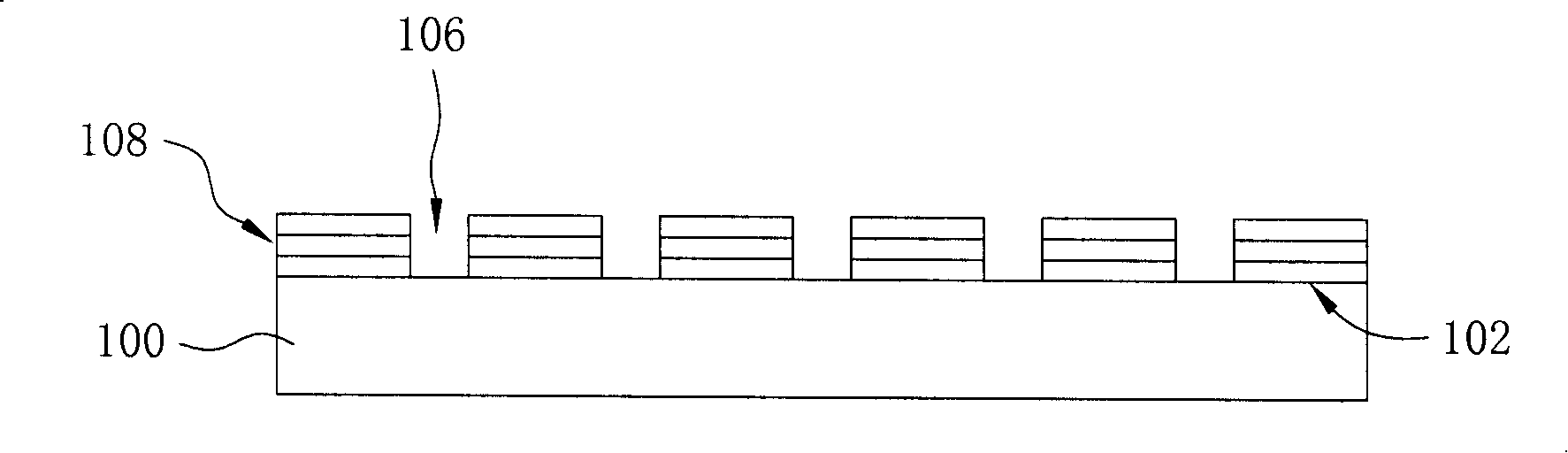
[0022] Please refer to Figure 1 to Figure 3 , which is a cross-sectional view showing the manufacturing process of a light emitting diode according to a preferred embodiment of the present invention. When fabricating a light emitting diode, a substrate 100 is firstly provided for epitaxial growth of a subsequent material layer thereon. Next, a reflective layer 104 is formed to completely cover the surface...
PUM
 Abstract
Description
Claims
Application Information