Reference current source circuit and infrared signal processing circuit
一种基准电流源、电流源的技术,应用在电子电路测试、非电信号传输系统、电路等方向,能够解决电路元件数增加等问题
- Summary
- Abstract
- Description
- Claims
- Application Information
AI Technical Summary
Problems solved by technology
Method used
Image

Examples
Embodiment approach 1
[0040] One embodiment of the present invention will be described below based on FIGS. 1 and 2 .
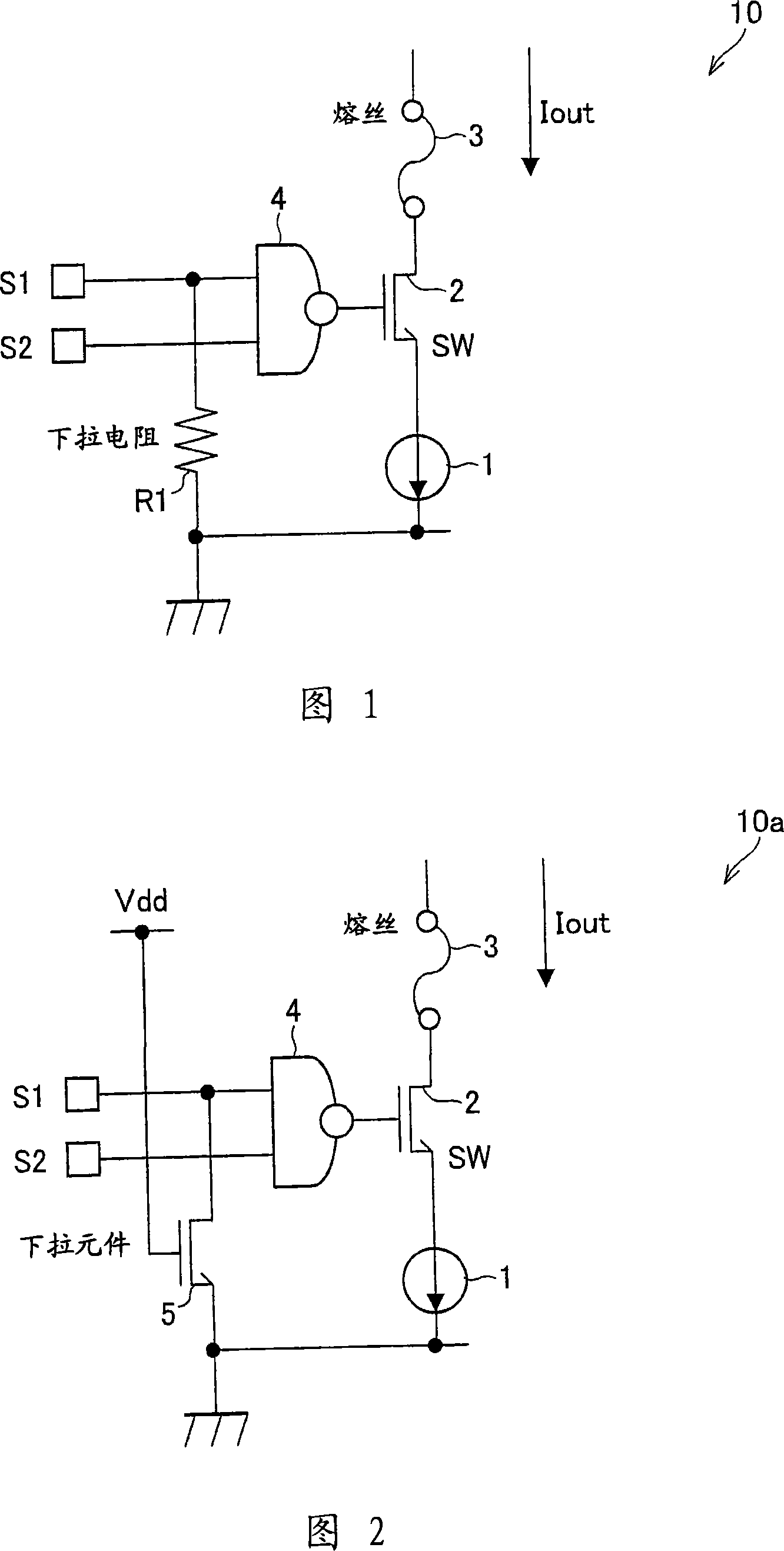
[0041] FIG. 1 shows the configuration of a reference current source circuit 10 for adjusting the characteristics of a semiconductor integrated circuit by fuse trimming.
[0042] The reference current source circuit 10 includes: a current source circuit 1; a switch circuit (SW) 2; a fine-tuning fuse (hereinafter simply referred to as a fuse) 3; a "NAND" circuit 4 (control circuit); and a pull-down resistor R1 (resistance sex element).
[0043] The switch circuit 2 has a function of connecting / disconnecting the current source circuit 1 and the fuse 3, and is composed of an N-channel MOS transistor. The drain of the MOS transistor is connected to an internal circuit of a semiconductor integrated circuit (not shown) through a fuse 3 , and the source of the MOS transistor is connected to a GND terminal through a current source circuit 1 . In addition, the gate of the above-mentioned ...
Embodiment approach 2
[0053] Another embodiment of the present invention will be described below based on FIG. 2 . Note that components, signals, and the like assigned the same reference numerals as those used in Embodiment 1 above have the same functions, and descriptions are not changed. In addition, here, only the points different from the reference current source circuit 10 will be described.
[0054] FIG. 2 shows a configuration of a reference current source circuit 10a for adjusting the characteristics of a semiconductor integrated circuit by fuse trimming.
[0055] The reference current source circuit 10a differs from the reference current source circuit 10 in that a pull-down element (resistive element) 5 is included instead of the pull-down resistor R1. Pull-down element 5 is composed of an N-channel type MOS transistor. The drain of the MOS transistor is connected to one input terminal of the NAND circuit 4 , the source is connected to the GND terminal, and the gate is connected to the ...
Embodiment approach 3
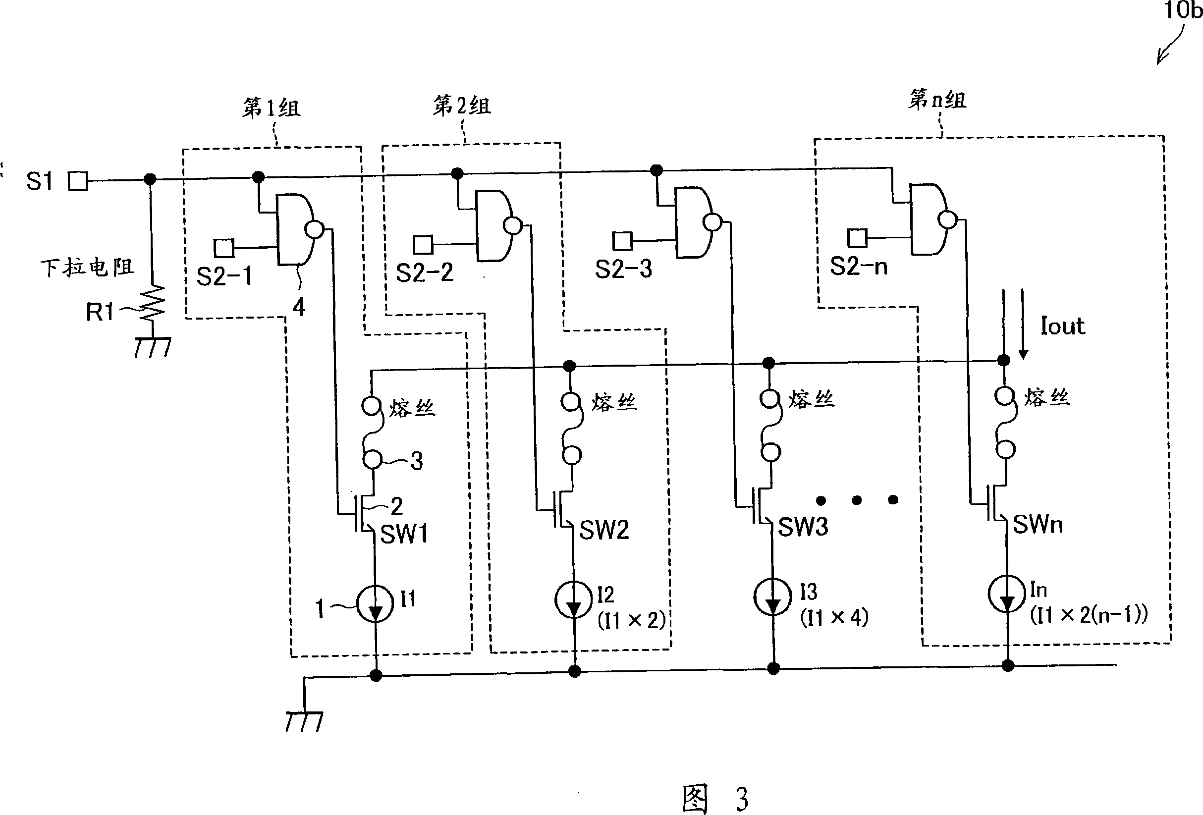
[0058] Another embodiment of the present invention is described below based on FIG. 3 and Table 3. Note that components, signals, and the like assigned the same reference numerals as those used in Embodiment 1 above have the same functions, and descriptions are not changed.
[0059] FIG. 3 shows a configuration of a reference current source circuit 10b for adjusting the characteristics of a semiconductor integrated circuit by fuse trimming.
[0060] The reference current source circuit 10b has the following structure: when the current source circuit 1, the switch circuit 2, the fuse 3 and the "NAND" circuit 4 in the reference current source circuit 10 are regarded as a group (set), it includes n This group of levels. One input terminal of each NAND circuit 4 in the n-stage group is connected to each other and shared, and the control signal S1 is input thereto. The control signal S2 (S2-1 to S2-n) is input to the other input terminal of each NAND circuit 4, respectively. The...
PUM
 Abstract
Description
Claims
Application Information
 - R&D
- Intellectual Property
- Life Sciences
- Materials
- Tech Scout
- Unparalleled Data Quality
- Higher Quality Content
- 60% Fewer Hallucinations
Browse by: Latest US Patents, China's latest patents, Technical Efficacy Thesaurus, Application Domain, Technology Topic, Popular Technical Reports.
© 2025 PatSnap. All rights reserved.Legal|Privacy policy|Modern Slavery Act Transparency Statement|Sitemap|About US| Contact US: help@patsnap.com