Stack type chip packaging structure and manufacturing method thereof

A technology of chip packaging structure and packaging structure, applied in semiconductor/solid-state device manufacturing, semiconductor/solid-state device components, semiconductor devices, etc. cost effect

Active Publication Date: 2008-07-23
ADVANCED SEMICON ENG INC
View PDF0 Cites 3 Cited by
  • Summary
  • Abstract
  • Description
  • Claims
  • Application Information

AI Technical Summary

Problems solved by technology

In this way, it is possible to overcome the problem of re-opening or modifying the original mold when filling the mold due to different chip sizes in the prior art.

Method used


Image

  • Stack type chip packaging structure and manufacturing method thereof
  • Stack type chip packaging structure and manufacturing method thereof
  • Stack type chip packaging structure and manufacturing method thereof

Examples


Embodiment Construction

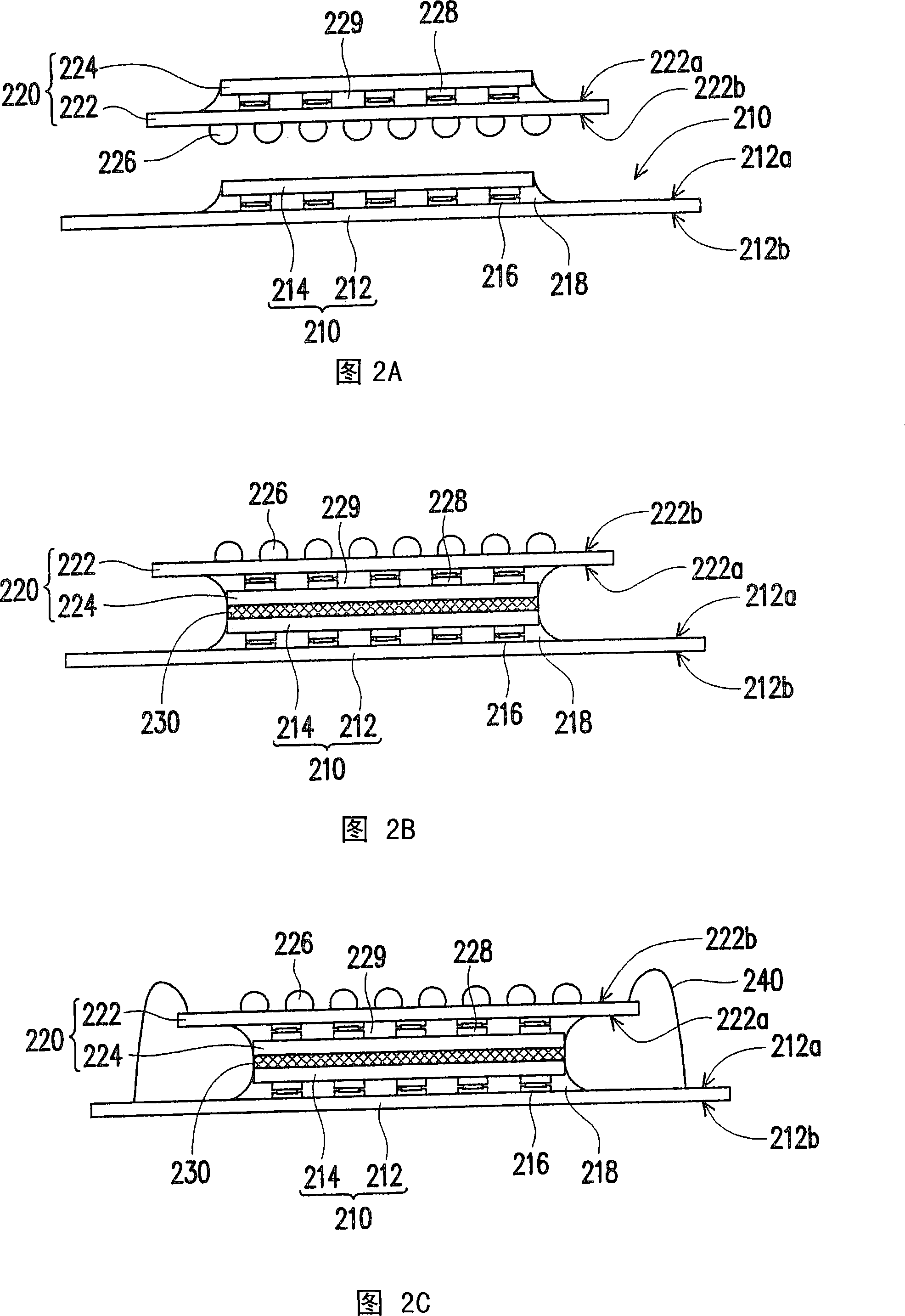
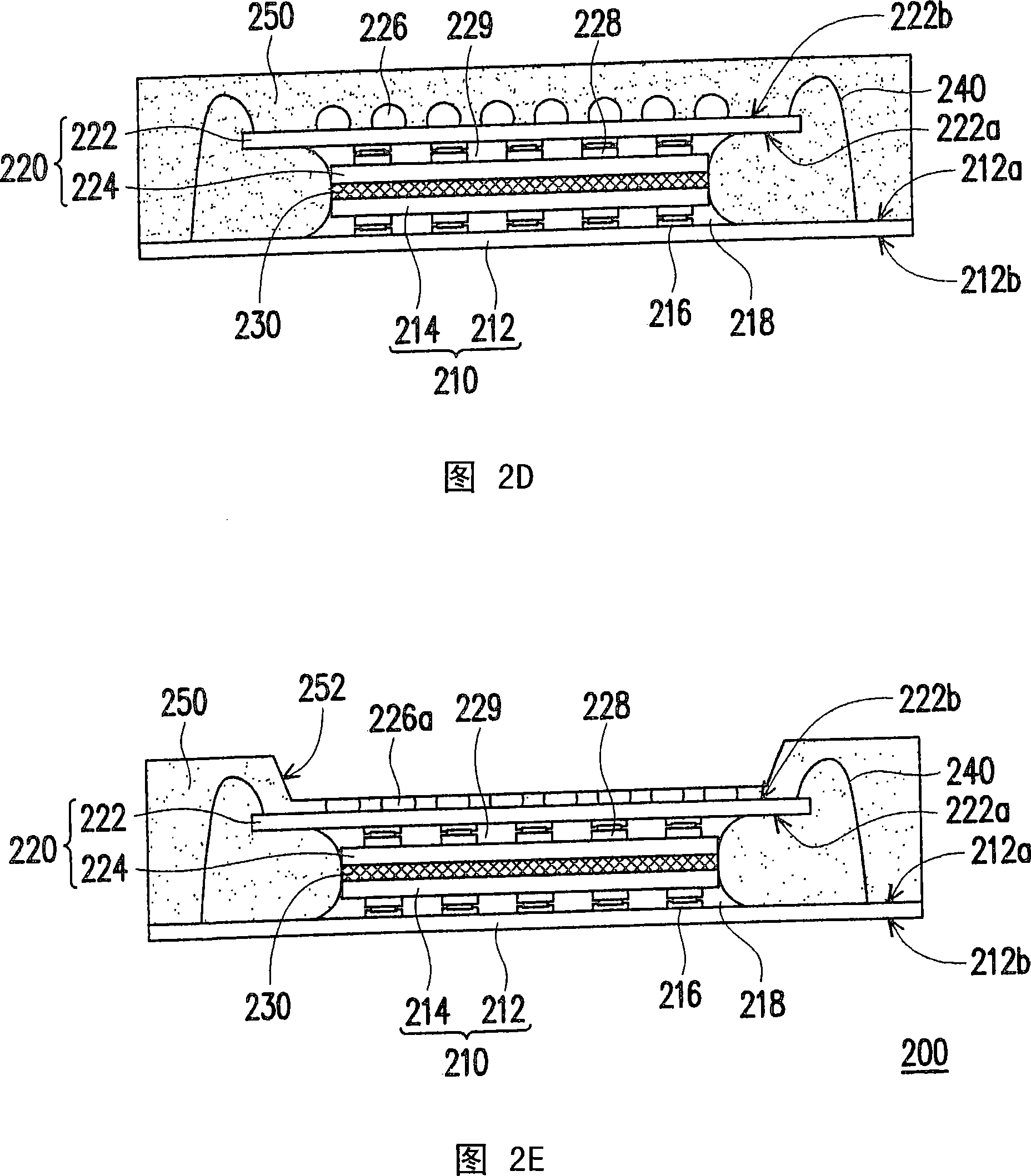
[0079] 2A-2H are schematic cross-sectional views showing a manufacturing process of a stacked chip packaging structure according to an embodiment of the present invention. First, as shown in FIG. 2A , a first packaging structure 210 and a second packaging structure 220 are provided. The first packaging structure 210 includes a first substrate 212 and a first chip 214 . The first substrate 212 has a first surface 212a and a second surface 212b corresponding thereto. The first chip 214 is disposed above the first surface 212 a of the first substrate 212 and is electrically connected to the first substrate 212 . In this embodiment, the first chip 214 is electrically connected to the first substrate 212 through a plurality of first bumps 216 . However, the first chip 214 may also be electrically connected to the first substrate 212 through other methods, which is not limited in the present invention. In addition, in order to protect the first bump 216 from damage and moisture, ...


PUM


Abstract

The invention relates to a stacked clip packaging structure, which comprises a first packaging structure, a second packaging structure and a first seal adhesive material, wherein the first packaging structure comprises a first substrate and a first clip which is stacked on the first substrate and is electrically connected with the first substrate. The second packaging structure is stacked on the first packaging structure, and comprises a second substrate, a second clip and a plurality of nuggets, the second clip is electrically connected with the second substrate, and the second substrate is electrically connected with the first substrate. The second clip is fixed on the first clip through an adhesion layer, and a plurality of nuggets are arranged on the back surface of the second substrate. The first seal adhesive material is arranged on the first substrate, the first packaging structure and the second packaging structure are coated by the first seal adhesive material, the first seal adhesive material is equipped with a concave portion, and the nuggets are exposed.

Description

technical field [0001] The invention relates to a chip packaging structure and a manufacturing method thereof, and in particular to a stacked chip packaging structure and a manufacturing method thereof. Background technique [0002] In today's information society, users are pursuing electronic products with high speed, high quality and multi-tasking performance. In terms of product appearance, the design of electronic products is also moving towards the trend of light, thin, short and small. In order to achieve the above purpose, many companies incorporate the concept of systemization when designing circuits, so that a single chip can have multiple functions, so as to save the number of chips configured in electronic products. In addition, as far as electronic packaging technology is concerned, in order to meet the design trend of light, thin, short, and small, the packaging design concept of multi-chip module (MCM), chip scale package (chip scale package, etc.) have also b...

Claims


Application Information

Patent Timeline
Patent Type & Authority Applications(China)
IPC IPC(8): H01L25/00H01L25/065H01L23/31H01L23/488H01L21/50H01L21/56H01L21/60
CPCH01L2225/1023H01L2225/1041H01L2225/1058H01L2225/1088H01L2924/15311H01L2924/1815H01L2924/19107H01L24/73H01L2224/16225H01L2224/32145H01L2224/32225H01L2224/48227H01L2224/73204H01L2224/73253H01L2224/73265H01L2924/00012H01L2924/00
Inventor 沈启智李政颖王维中
Owner ADVANCED SEMICON ENG INC
Why Eureka
Try Eureka