High-pressure solid phase crystallization method

A polysilicon thin film and thin film thickness technology, which is applied in the field of solar cell material preparation, can solve problems such as hindering the industrialization of polysilicon thin film photovoltaic technology.

Inactive Publication Date: 2008-08-06
BEIJING XINGZHE MULTIMEDIA TECH
View PDF0 Cites 5 Cited by
  • Summary
  • Abstract
  • Description
  • Claims
  • Application Information

AI Technical Summary

Problems solved by technology

This cumbersome, complicated and lengthy process hinders the in

Method used


Image

  • High-pressure solid phase crystallization method

Examples


Embodiment Construction

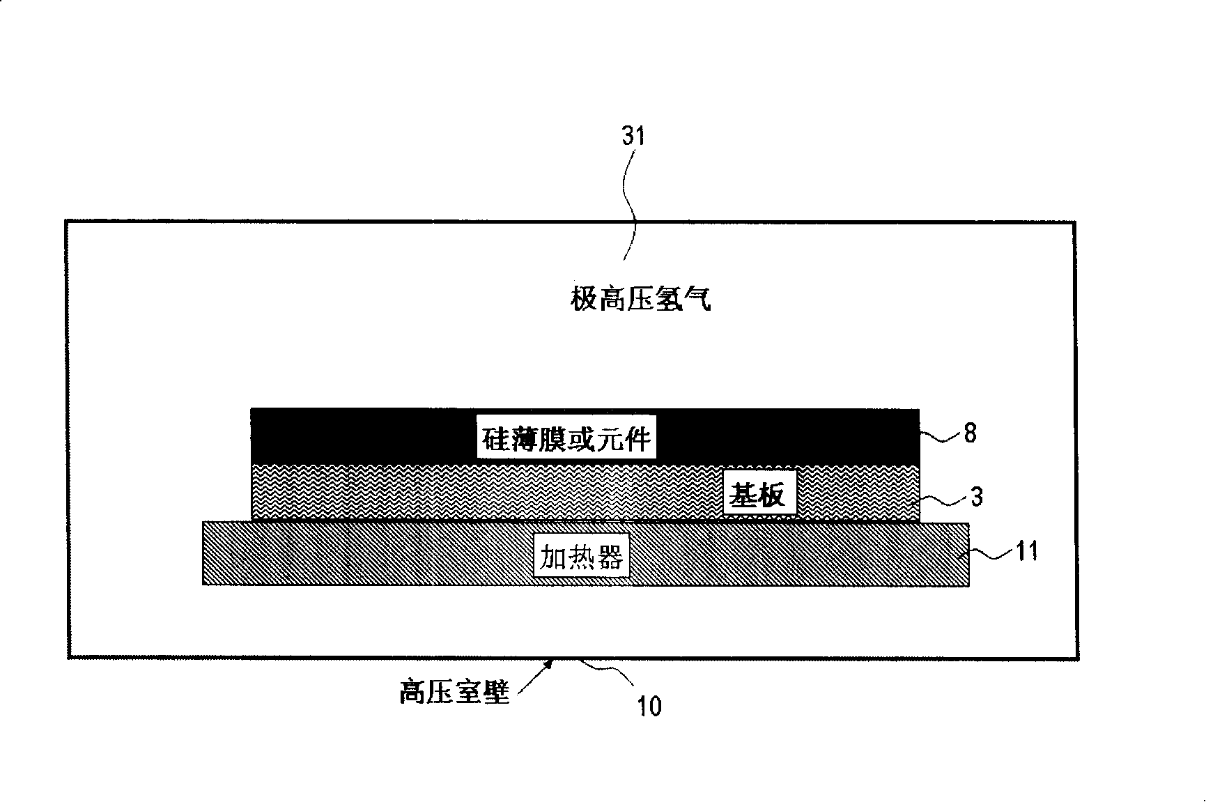
[0009] Use plasma-enhanced chemical vapor deposition equipment to form hydrogenated amorphous silicon with a thickness not exceeding 5 microns on a substrate 3 at a temperature not exceeding 300°C, and then place the material in a sealable high-temperature and high-pressure processing device 10 Place the hydrogenated amorphous silicon film or its element 8 deposited on the substrate 3 on a support base 11 with a heating function, introduce a gas whose main component contains hydrogen 31 into the box, and make its pressure reach no less than 200 Atmospheric high pressure, preferably not less than 1000 atmospheres, and maintain the substrate temperature at not lower than 600°C. In this high temperature and high pressure state, it is maintained for 2-20 hours.


PUM


Abstract

The invention discloses a method for changing an amorphous silicon thin film into a polycrystalline silicon thin film, which comprises the following steps: placing hydrogenated amorphous silicon thin film or a device of the method which are deposited on a base plate into the high pressure hydrogen gas environment with no less than two hundred atmospheric pressure, and maintaining 2-20h under the temperature which is no lower than 600 DGE C, the obtained hydrogen deactivation polycrystalline silicon thin film can be directly used as highly effective photoelectric conversing material.

Description

technical field [0001] The invention belongs to the field of semiconductor material preparation, and in particular relates to the preparation technology of solar cell materials. Background technique [0002] Solar photovoltaic power generation is one of the important ways to obtain renewable energy that is beneficial to the environment. Today's photovoltaic market is dominated by crystalline silicon products, that is, wafer-based photovoltaic modules including monocrystalline silicon and polycrystalline silicon. This is due to the fact that today's thin-film photovoltaic products have not yet reached a price-performance ratio that can compete with crystalline silicon. The reason It is often because its photoelectric conversion efficiency is lower than that of crystalline silicon products, and its production cost per unit of power generation cannot be significantly lower than that of crystalline silicon products. [0003] Thin-film polycrystalline silicon is the most potenti...

Claims


Application Information

Patent Timeline
IPC IPC(8): C30B1/12C30B28/02C30B29/06H01L31/18
CPCY02P70/50
Inventor 李沅民马昕
Owner BEIJING XINGZHE MULTIMEDIA TECH
Why Eureka
Try Eureka