Liquid crystal display panel, pixel structure and method of manufacture

A pixel structure and manufacturing method technology, which is applied in semiconductor/solid-state device manufacturing, optics, instruments, etc., can solve the problems of rising manufacturing costs, reducing the light-transmitting part of the pixel area, reducing the pixel aperture ratio, etc., to achieve a reduction in the aperture ratio , Reduce the effect of color cast problem

Active Publication Date: 2008-08-06
NANJING CEC PANDA LCD TECH
View PDF1 Cites 25 Cited by
  • Summary
  • Abstract
  • Description
  • Claims
  • Application Information

AI Technical Summary

Problems solved by technology

The existing technology uses capacitive coupling to realize this multi-domain technology, but the current capacitive coupling technology is usually a capacitive coupling layer formed at the same time as the first conductive metal is formed, so the capacitive coupling layer is an opaque metal, which leads to pixel The area that can transmit light is reduced, thereby reducing the aperture ratio of the pixel, which leads to an increase in manufacturing costs

Method used


Image

  • Liquid crystal display panel, pixel structure and method of manufacture
  • Liquid crystal display panel, pixel structure and method of manufacture
  • Liquid crystal display panel, pixel structure and method of manufacture

Examples


Embodiment Construction

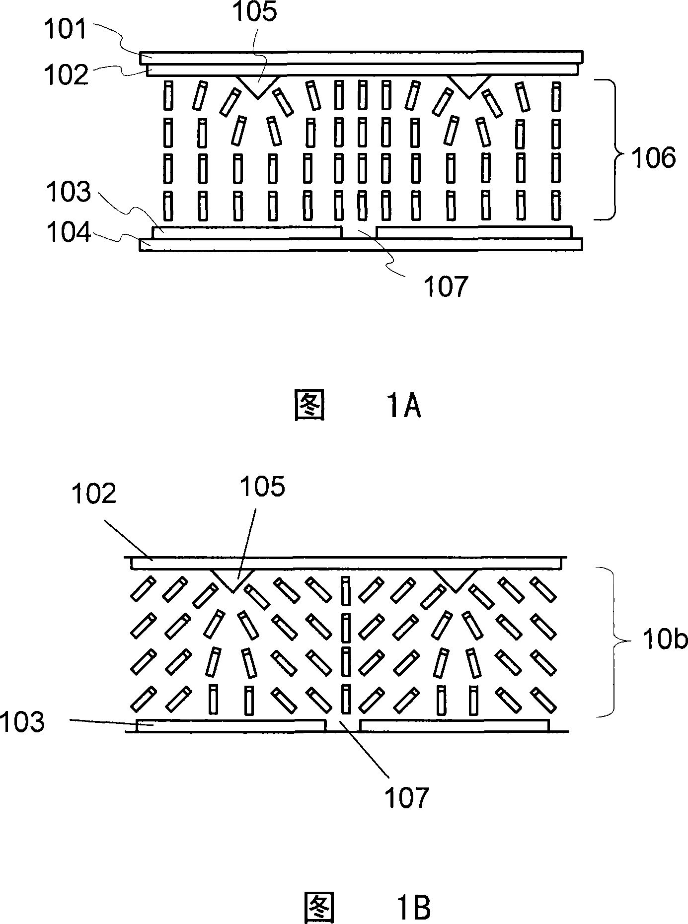
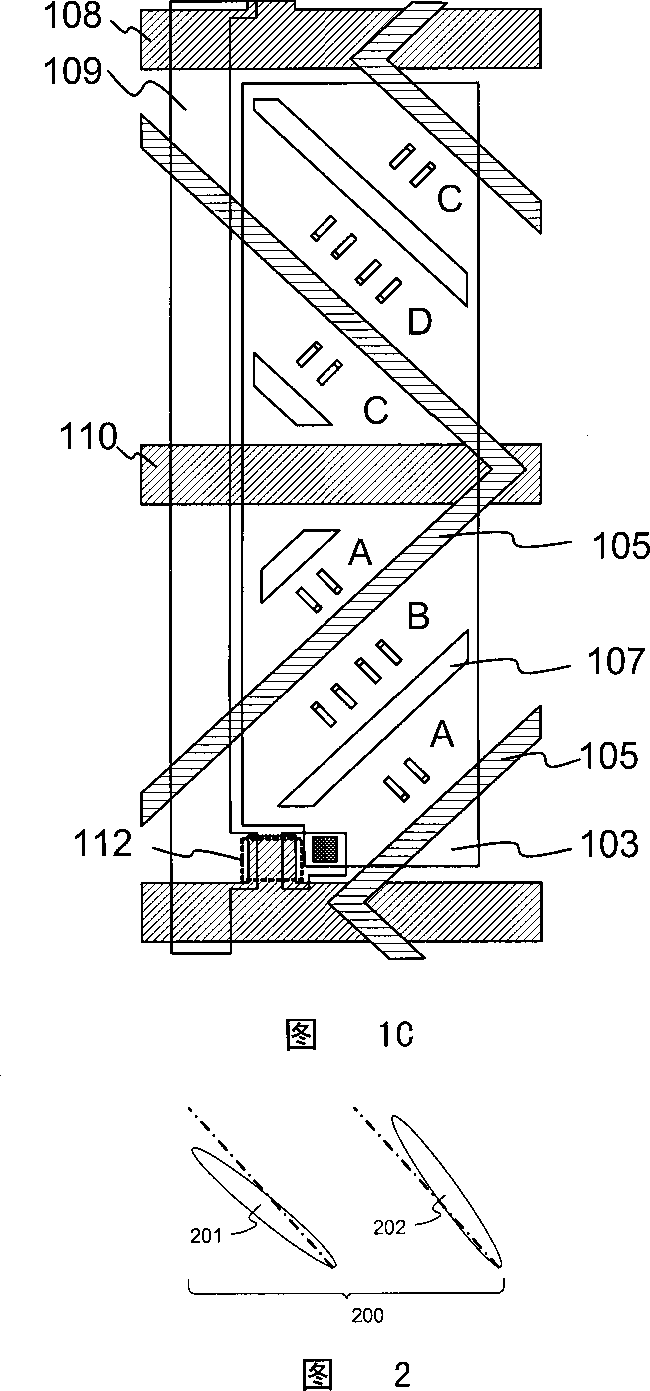
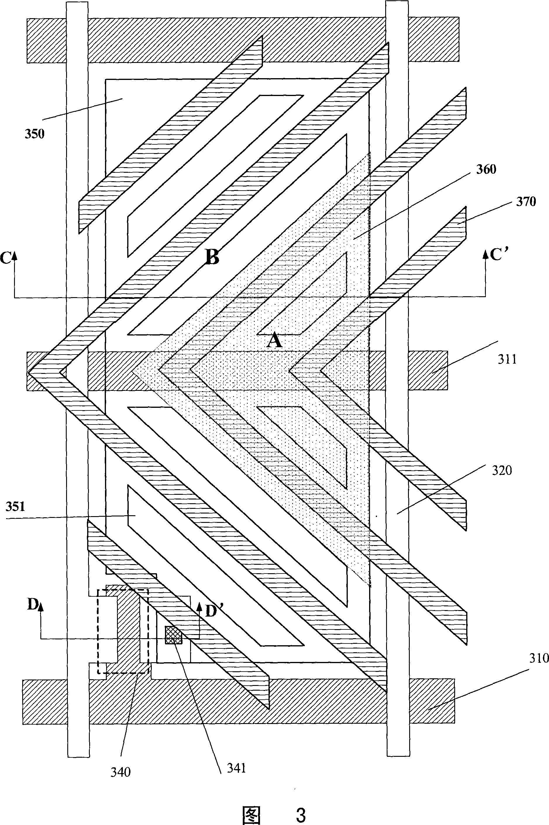
[0028] FIG. 3 shows a pixel structure suitable for a multi-domain vertical alignment mode liquid crystal display device of the present invention, which includes scan lines 310, data lines 320, TFT 340, and pixels arranged on a thin film transistor array substrate (not shown). An electrode 350, and a coupling capacitor dielectric layer 360. Two adjacent scan lines 310 and two adjacent data lines 320 define a pixel area. This pixel area is further divided into a first sub-pixel area A and a second sub-pixel area B.

[0029] The pixel electrode 350 has a slit pattern composed of a plurality of slits 351, and the pixel electrode 350 is connected to the source of the TFT 340 through the contact hole 341, the gate of the TFT 340 is connected to the scanning line 310, and the drain of the TFT 340 is connected to the data line 320 .

[0030] The above-mentioned pixel structure is arranged on a thin film transistor array substrate, on which a common electrode line 311 is arranged, an...


PUM


Abstract

The present invention relates to a pixel structure suitable for liquid crystal display devices in a multidomain vertical tropism mode. The pixel structure comprises a scan line, a data line, a thin film transistor and a pixel electrode. The scan line and the data line define a pixel region which comprises a first sub-pixel region and a second sub-pixel region. The thin film transistor is arranged on a substrate and electrically connected to the scan line and the data line; the pixel electrode is arranged within the pixel region and electrically connected to the source electrode of the thin film transistor, wherein the height of part pixel electrodes in the first sub-pixel region is lower than the height of part pixel electrodes in the second sub-pixel region, and a layer of transparent first coupling capacitance medium layer is covered at least on the pixel electrode of the first sub-pixel region. The present invention further discloses a method for manufacturing the pixel structure and a liquid crystal display panel.

Description

technical field [0001] The invention relates to a thin film transistor liquid crystal display device (TFT-LCD). In particular, it relates to a display panel of a multi-domain vertical alignment mode liquid crystal display device, a pixel structure and a manufacturing method thereof. Background technique [0002] At present, liquid crystal displays with superior characteristics such as high image quality, good space utilization efficiency, low power consumption, and no radiation have gradually become the mainstream of the market. In order to allow users to have better display quality, current LCD monitors are all oriented toward high contrast ratio, no gray scale inversion, little color shift, and high luminance. , high color saturation, fast response and wide viewing angle to develop. [0003] The liquid crystals in liquid crystal display devices do not emit light by themselves. Liquid crystal display uses an electric field to control the twisting of liquid crystal molecu...

Claims


Application Information

Patent Timeline
Patent Type & Authority Applications(China)
IPC IPC(8): G02F1/139G02F1/1362H01L27/12H01L21/84
Inventor 李喜峰
Owner NANJING CEC PANDA LCD TECH
Why Eureka
Try Eureka