Method for manufacturing thin membrane silicon electrooptical device with single-chamber plasma case

A plasma box and photoelectric conversion technology, which is applied in the manufacture of electrical components, semiconductor devices, semiconductor/solid-state devices, etc., can solve the problems of non-interchangeable use, limitation and productivity, etc.

Inactive Publication Date: 2008-08-20
BEIJING XINGZHE MULTIMEDIA TECH
View PDF0 Cites 14 Cited by
  • Summary
  • Abstract
  • Description
  • Claims
  • Application Information

AI Technical Summary

Problems solved by technology

Such multiple vacuum chambers cannot be used interchangeab

Method used


Image

  • Method for manufacturing thin membrane silicon electrooptical device with single-chamber plasma case
  • Method for manufacturing thin membrane silicon electrooptical device with single-chamber plasma case
  • Method for manufacturing thin membrane silicon electrooptical device with single-chamber plasma case

Examples


Embodiment Construction

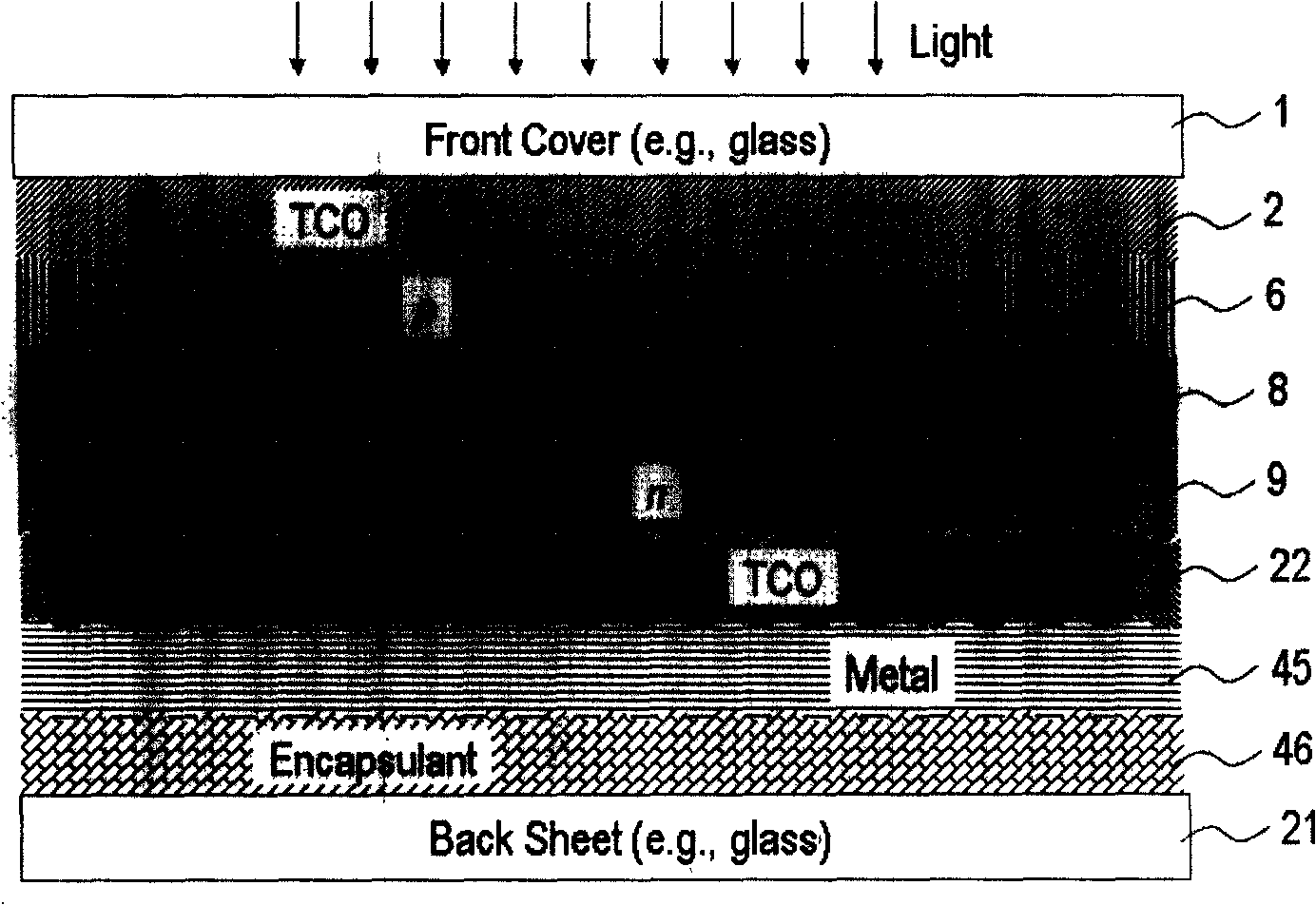
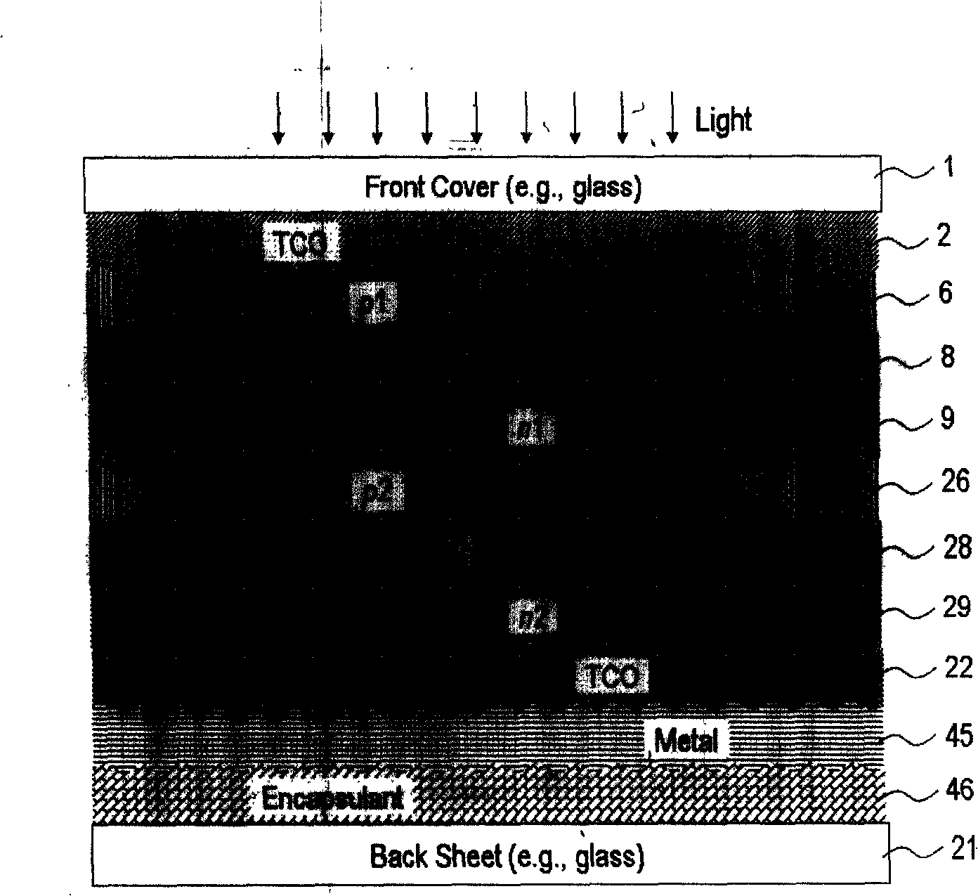
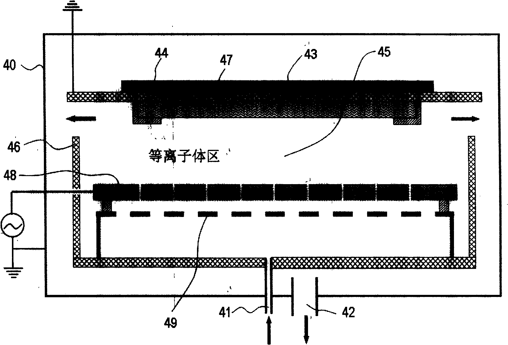
[0032] process Figure 5 shows a typical production procedure for employing Figure 4 The PECVD system shown fabricates a stacked double-junction thin-film silicon p-i-n photoelectric device (eg figure 2 shown). This production step is described below as an application example of the present invention. In the first step S1, the glass substrate 3 coated with the tin oxide front electrode is put into the plasma box 20 fixedly placed in the single vacuum chamber 10 which is preheated to a temperature higher than 200°C. In the second step S2, the vacuum chamber is evacuated by a dry pump to make the air pressure lower than 8×10 -6 mbar. At the same time, the heating power of the vacuum chamber 10 is adjusted so that the temperature inside the vacuum chamber (including the temperature inside the plasma box 20 ) is stably maintained at a predetermined value between 160°C and 260°C. A number of temperature sensors are placed at various points inside the vacuum chamber 10, inclu...


PUM


Abstract

The invention discloses a device and a method for the production of a thin-film silicon optical-to-electrical transducer. A plasma enhanced chemical vapor deposition system (PECVD) used in the invention consists of a single vacuum chamber and a plasma chamber carrying a plurality of base plates in the vacuum chamber. The preparation method of the p-i-n optical-to-electrical transducer based on hydrogenated silicon films comprises the steps as follows: a p-type, an i-type and an n-type thin-film silicon layer sequentially generated on most of the base plates in the same plasma chamber are fixedly arranged in the same vacuum chamber. In the deposition process of each film layer, the device is not required to be cleaned and no cross contamination of the i layer is caused. The steps can be repetitively processed in the same base plates to obtain a multi-junction optoelectronic device. The method for the production of thin-film the silicon optical-to-electrical transducer has incomparable advantages of low cost and high productivity.

Description

technical field [0001] The invention belongs to the production field of photoelectric conversion devices, and in particular relates to a manufacturing device and method for greatly improving the productivity of hydrogenated silicon thin film photoelectric conversion devices and reducing their cost. Background technique [0002] In recent years, the development of thin-film photoelectric conversion (photovoltaic) cells and large-area templates has received worldwide attention. Especially hydrogenated amorphous silicon (a-Si) and nanocrystalline silicon (nc-Si) have shown great potential to play a pivotal role in applications such as building-integrated photovoltaics. An important feature of thin-film silicon photoelectric conversion devices (commonly known as solar photovoltaic cells and templates) formed at a relatively low temperature below 260°C is the use of well-established industrial coating equipment and procedures, by depositing silicon semiconductors and The film la...

Claims


Application Information

Patent Timeline
IPC IPC(8): C23C16/513C23C16/30C23C16/52H01L21/205H01L31/0216H01L31/0264
Inventor 李沅民马昕
Owner BEIJING XINGZHE MULTIMEDIA TECH
Why Eureka
Try Eureka