Electronic packaging structure
A technology for electronic packaging and electronic components, which is applied to circuits, electrical components, electrical solid devices, etc., can solve the problems of large volume, low space utilization rate of the printed circuit board 110 and the packaging substrate 210, etc., and achieve the effect of high density
- Summary
- Abstract
- Description
- Claims
- Application Information
AI Technical Summary
Problems solved by technology
Method used
Image

Examples
no. 1 example
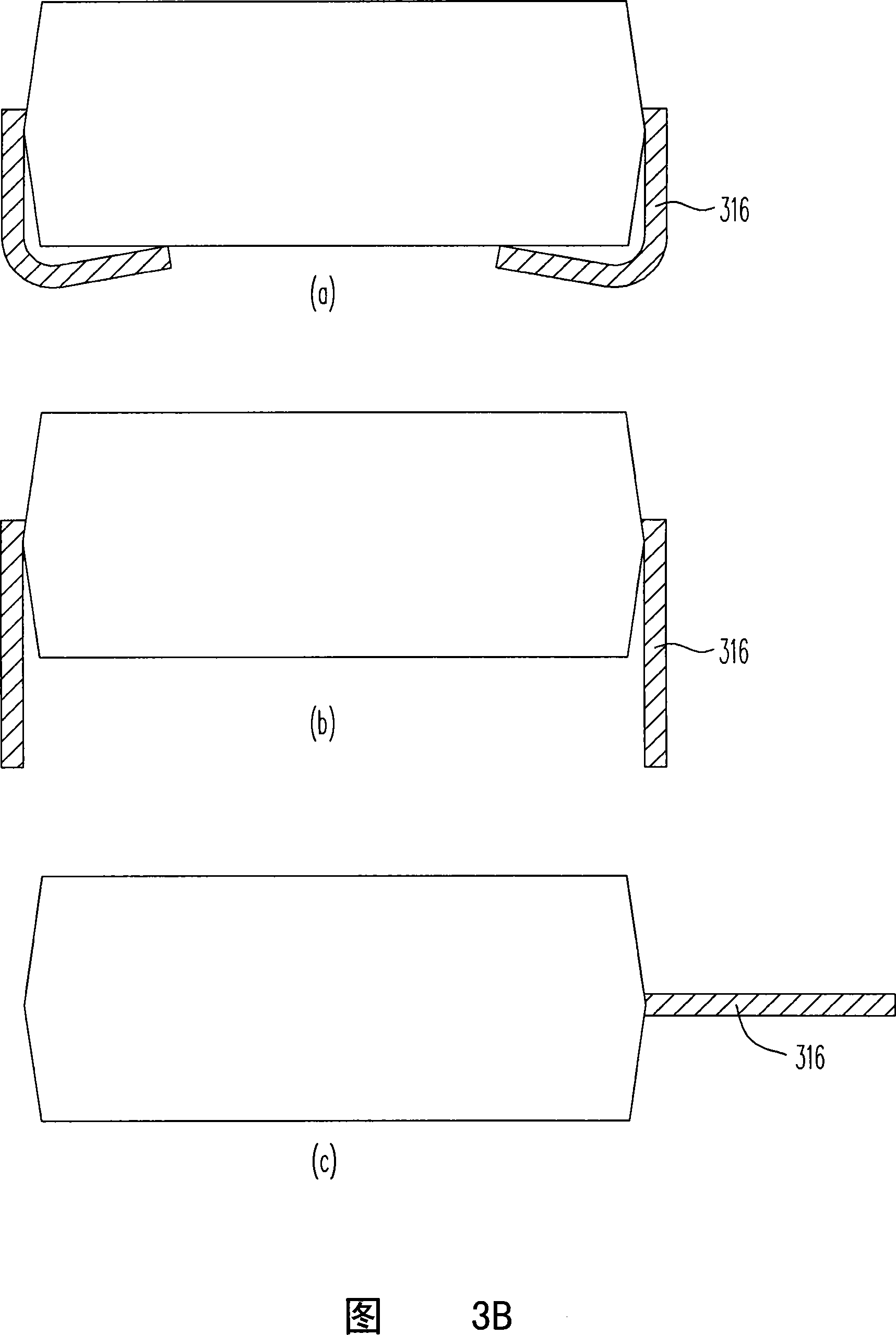
[0045] Please refer to FIG. 3A , which is a schematic cross-sectional view of an electronic packaging structure according to the first embodiment of the present invention. The electronic packaging structure 300 of the first embodiment includes a first carrier 310, at least one first electronic component 320 (four are schematically shown in FIG. 3A ), and at least one second electronic component 330 (one is schematically shown in FIG. 3A ). ) with a colloid 340. The first carrier 310 has a first carrying surface 312 and a second carrying surface 314 opposite to each other. The first electronic components 320 are disposed on the first carrying surface 312 and electrically connected to the first carrier 310 . The second electronic component 330 is disposed on the second carrying surface 314 and electrically connected to the first carrier 310 .
[0046]In this embodiment, the volume of the second electronic component 330 may be greater than that of the first electronic component...
no. 2 example
[0055] Please refer to FIG. 4 , which is a schematic cross-sectional view of an electronic packaging structure according to a second embodiment of the present invention. The difference between the electronic packaging structure 400 of the second embodiment and the electronic packaging structure 300, 300' of the first embodiment is that the electronic packaging structure 400 further includes a second carrier 460, and the number of the first electronic components 420 is Multiple. Some of these first electronic components 420 are disposed on the second carrier 460 and electrically connected to the second carrier 460, and the second carrier 460 is disposed on the first carrying surface 412 of the first carrier 410 and electrically connected to the first carrier 410 . In other words, in this embodiment, some of these first electronic components 420 are indirectly disposed on the first carrying surface 412, and the rest of these first electronic components 420 (only the rightmost f...
no. 3 example
[0059] Please refer to FIG. 5 , which is a schematic cross-sectional view of an electronic packaging structure according to a third embodiment of the present invention. In the electronic package structure 500 of the third embodiment, the second carrier 560 such as a circuit board is disposed on the first carrier surface 512 of the first carrier 510 such as a lead frame and is electrically connected to the first carrier 510. There are multiple first electronic components 520 , and these first electronic components 520 are indirectly disposed on the first carrying surface 512 through the second carrier 560 . As far as the relative positions shown in FIG. 5 are concerned, the first electronic components 520 disposed on the second carrier 560 are respectively resistors, capacitors, logic control elements, capacitors and resistors from left to right. In addition, there are multiple second electronic components 530, and these second electronic components 530 arranged on the second ...
PUM
 Abstract
Description
Claims
Application Information
 - R&D
- Intellectual Property
- Life Sciences
- Materials
- Tech Scout
- Unparalleled Data Quality
- Higher Quality Content
- 60% Fewer Hallucinations
Browse by: Latest US Patents, China's latest patents, Technical Efficacy Thesaurus, Application Domain, Technology Topic, Popular Technical Reports.
© 2025 PatSnap. All rights reserved.Legal|Privacy policy|Modern Slavery Act Transparency Statement|Sitemap|About US| Contact US: help@patsnap.com