Electromagnetic radiation decoupler
A decoupler, electronic device technology, applied in the field of electromagnetic radiation isolation or attenuation devices, can solve the problems of increasing cost and complexity, complex antenna design, etc.
- Summary
- Abstract
- Description
- Claims
- Application Information
AI Technical Summary
Problems solved by technology
Method used
Image
Examples
example 1
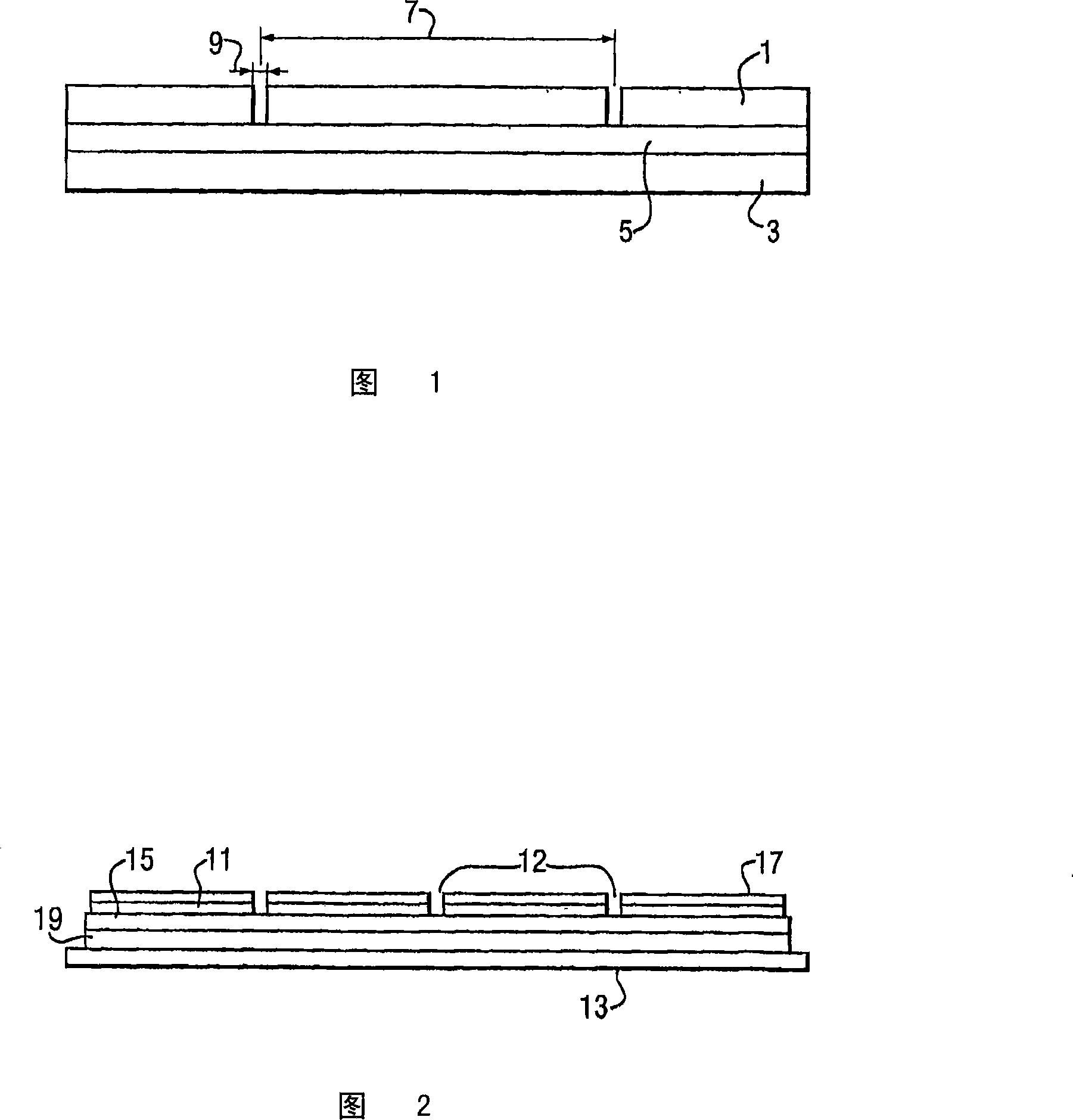
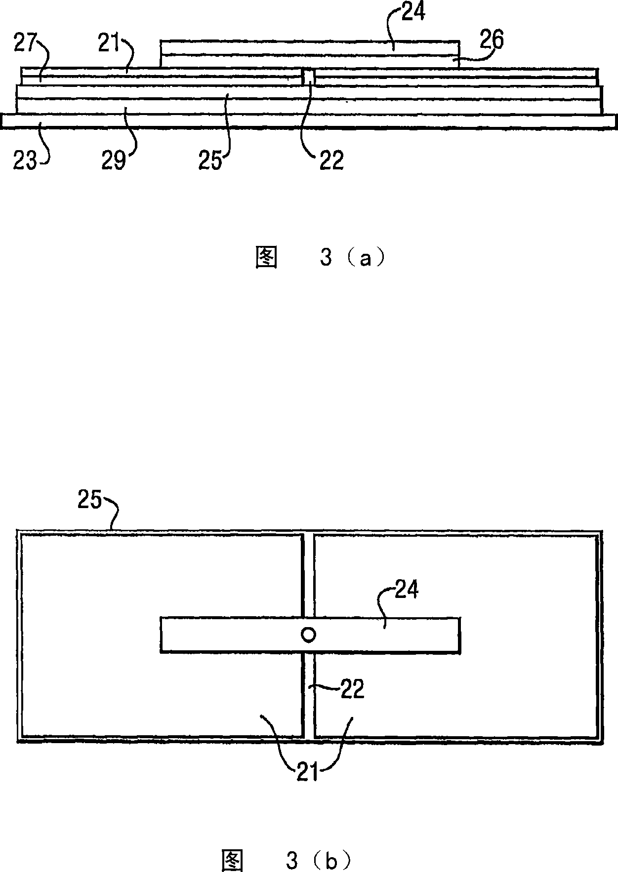
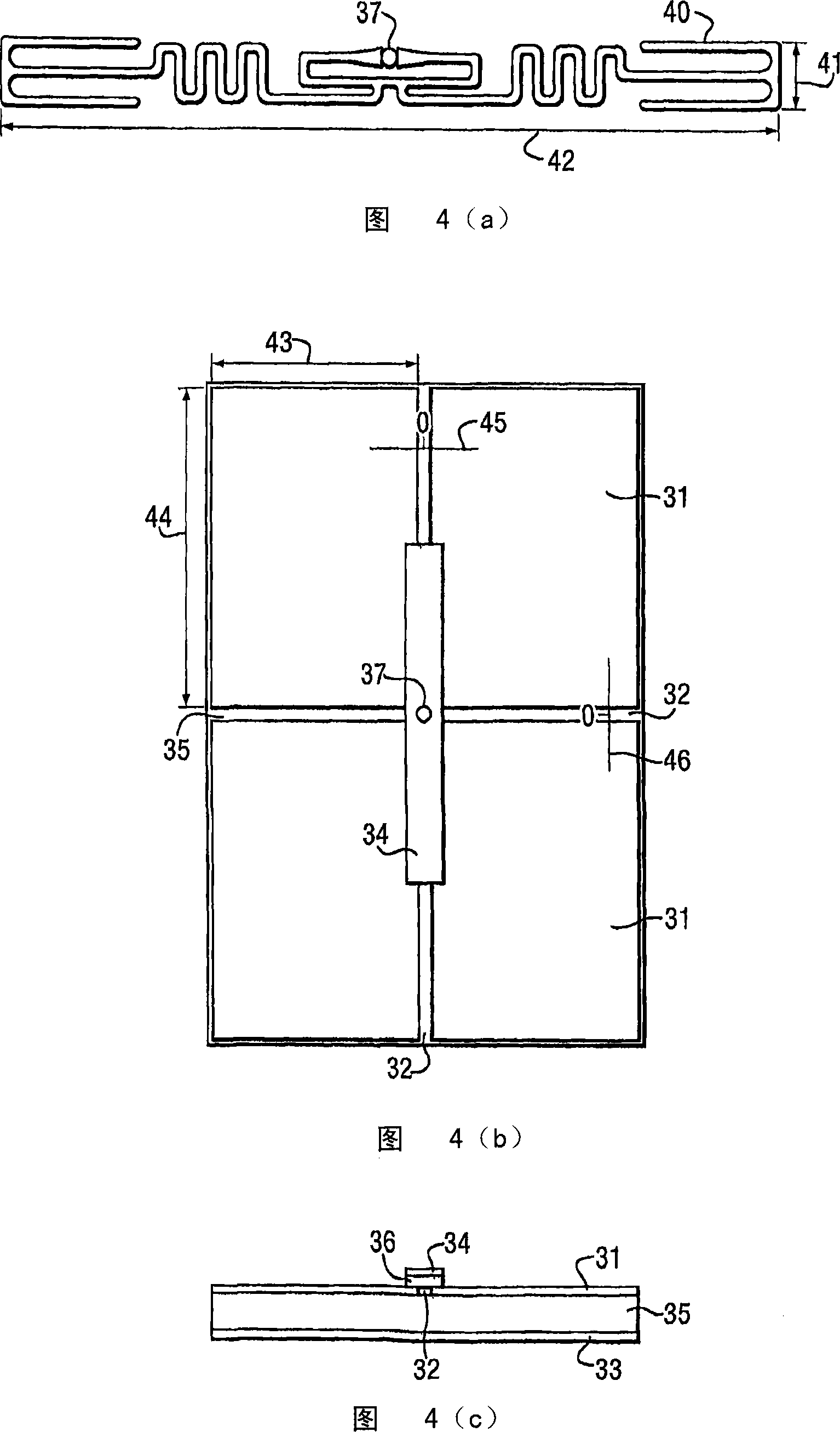
[0210]Adopt non-conductive catalyst ink (provided by Sun Chemical, product name is QS1, QS2 or DP1607, as disclosed in application GB 0422386.3) will decoupling unit, promptly first and second conductor layer screen print (double-sided) to on a polymer (forming the dielectric core) with known electrical properties. The dimensions of the UHF decoupler depend on the electrical properties and thickness of the polymer. For example, using Quinn plastic, Spectar-grade PETG sheets with a thickness of 1 mm, a relative permittivity of 3.2, results in a decoupler period of 95 mm and a minimum decoupler length of 190 mm (using island length ≈λ / (2√ (dielectric constant), wherein the refractive index is approximately equal to the root of the dielectric constant). The decoupler pattern is printed on the front side of the polymer, that is, by two orthogonal Four equal-sized islands separated by lines. Print the reverse side of the decoupler as a solid area.
[0211] The ink was cured by he...
example 2
[0214] Decoupling cells (both sides) are screen printed onto polymers with known electrical properties using conductive inks, eg, Acheson Electrodag PR401B Carbon ink or Acheson Electrodag 503 Silver ink. The dimensions of the UHF decoupler depend on the electrical properties and thickness of the polymer. For example, using Quinn plastic, Spectar-grade PETG sheet with a thickness of 1 mm, has a relative permittivity of 3.2, resulting in a decoupler period of 95 mm and a minimum decoupler length of 190 mm. The polymer was printed on the front side in a decoupler pattern and the back side was printed as a solid area.
[0215] The ink was cured (for Acheson Electrodag PR401B Carbon ink and Acheson Electrodag 503 Silver ink) by heating the sample, which allowed the ink to solidify and adhere to the substrate.
[0216] Afterwards, the resulting product was laminated with a functional spacer and mounted on a decoupler in the same manner as defined in Example 1.
example 3
[0218] An etch resist (eg, Sun Chemical XV 750) is screen printed onto the metal surface using a polymer film (eg, DuPont Mylar PET film) covering the metal. Once dry, the etch resist adheres to the surface of the metal in a pattern of decouplers. Afterwards, the film is placed in a caustic solution (e.g., in MAX ETCH from Old Bridge Chemicals). TM within 20R). This process removes uncovered metal areas, leaving only the non-conductive substrate. Afterwards, the metallized patterned film is laminated onto the core material and sandwiched by another metallized non-patterned film used as a backplane. Afterwards, it requires spacer lamination and labeling as defined in Example 1 and Example 2.
PUM
| Property | Measurement | Unit |
|---|---|---|
| Slit width | aaaaa | aaaaa |
| Thickness | aaaaa | aaaaa |
Abstract
Description
Claims
Application Information


