Imaging device and image processing method

A camera device and image signal technology, which is applied in image communication, TV, color TV parts, etc., can solve the problems of cost increase, lens enlargement, amplification noise, etc., and achieve cost reduction, simplification of optical system, and noise impact small effect

Inactive Publication Date: 2008-09-03
KYOCERA CORP
View PDF2 Cites 16 Cited by
  • Summary
  • Abstract
  • Description
  • Claims
  • Application Information

AI Technical Summary

Problems solved by technology

[0021] Therefore, regardless of the single focus lens, even in lenses such as zoom systems and AF systems, due to the high precision of optical design and the resulting increase in cost, there are still serious problems in use.
[0022] In other words, in the existing imaging devices, proper convolution calculations cannot be performed, and the required optical design is to eliminate astigmatism and coma that cause deviations in spot (SPOT) images at wide angle (Wide) and telephoto (Tele). aberration, zoom chromatic aberration and other aberrations
[0023] However, the optical design that eliminates these aberrations increases the difficulty of optical design, and causes problems such as increased design man-hours, increased costs, and enlarged lenses.
[0024] In addition, in the devices disclosed in the above-mentioned documents, for example, when photographing in a dark place, when the image is restored by signal processing, the noise is also amplified at the same time.
[0025] Therefore, in an optical system that includes an optical system and signal processing such as the above-mentioned phase plate and other optical wavefront modulation elements and subsequent signal processing, when imaging in a dark place, the disadvantage is that the magnification Noise, affecting the restored image

Method used


Image

  • Imaging device and image processing method
  • Imaging device and image processing method
  • Imaging device and image processing method

Examples


Embodiment Construction

[0081] Hereinafter, embodiments of the present invention will be described with reference to the drawings.

[0082] FIG. 3 is a block configuration diagram showing an embodiment of the imaging device of the present invention.

[0083] The imaging device 100 of this embodiment includes an optical system 110, an imaging element 120, an analog front end (AFE) 130, an image processing device 140, a camera signal processing unit 150, an image display memory 160, an image monitoring device 170, and an operation unit 180. , and the exposure control device 190 .

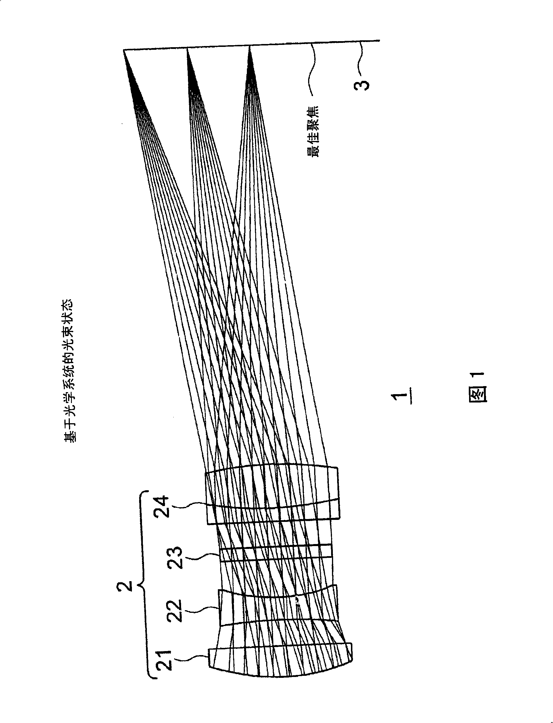
[0084] The optical system 110 supplies an image of the subject OBJ to the imaging element 120 .

[0085] The imaging element 120 is composed of a CCD or a CMOS sensor. The CCD and the CMOS sensor image the image acquired by the optical system 110, and output the primary image signal FIM as an electrical signal to the image processing through the analog front-end part 130. device 140.

[0086] In FIG. 3 , as an example, th...


PUM


Abstract

There are provided an imaging device and an image processing method capable of simplifying an optical system, reducing cost, and obtaining a restored image having a small noise affect. The imaging device includes an optical system (110) and an imaging element (120) for forming a primary image and an image processing device (140) for forming the primary image into a highly fine final image. In the image processing device (140), filter processing is formed for an optical transfer function (OTF) in accordance with exposure information from an exposure control device (190).

Description

technical field [0001] The present invention relates to an imaging device such as a digital camera using an imaging element and equipped with an optical system, a camera mounted on a mobile phone, a camera mounted on a portable information terminal, an image inspection device, an industrial camera for automatic control, and an image processing method. Background technique [0002] In recent years, along with the digitization of information that has been rapidly advanced, correspondingly, the video field is extremely remarkable. [0003] In particular, a CCD (Charge Coupled Device) or a CMOS (Complementary Metal Oxide Semiconductor) sensor, which is a solid-state imaging element, is often used as an imaging surface instead of a conventional film, as typified by a digital camera. [0004] In this way, an imaging lens device using a CCD and a CMOS is used in an imaging element to optically acquire an image of a subject by an optical system, and extract it as an electrical signa...

Claims


Application Information

Patent Timeline
Patent Type & Authority Applications(China)
IPC IPC(8): H04N5/232H04N5/225
Inventor 林佑介村濑成康
Owner KYOCERA CORP
Why Eureka
Try Eureka