Probe assembling

A probe and contact member technology, applied in the field of probe assembly, can solve the problems of difficulty in exposing the surface of the electrode block, damage to the circuit of the electrode block, damage to the surface of the electrode block, etc., to achieve the effect of reliable electrical connection and reduce the contact resistance.

Inactive Publication Date: 2008-09-10
木本军生
View PDF2 Cites 3 Cited by
  • Summary
  • Abstract
  • Description
  • Claims
  • Application Information

AI Technical Summary

Problems solved by technology

[0016] However, it is extremely difficult to only remove the oxide film of the film and expose the surface of the electrode block, and the friction action will not only remove the oxide film, but also cut off the electrode block, which may cause damage to the surface of the electrode block and cause In the follow-up project, there may be problems such as poor bonding and wiring, or damage to the circuit at the bottom of the electrode block; in addition, when cutting the aluminum and other materials of the electrode block, after being placed for a long time in the state attached to the top of the probe, it has been attached The aluminum oxidizes, forming a tenacious deposit that cannot be removed until the next inspection, even by rubbing action

Method used


Image

  • Probe assembling
  • Probe assembling
  • Probe assembling

Examples


Embodiment 1

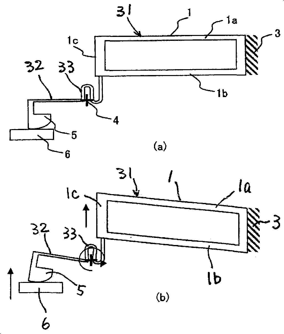
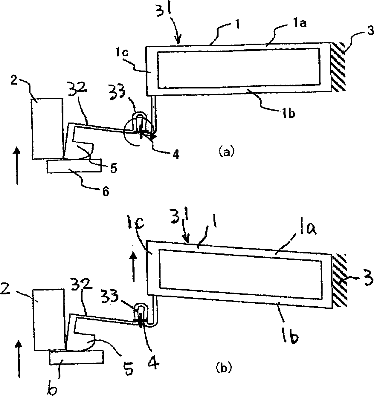
[0045] figure 1 It is a side view of the assembled probe of the first embodiment of the present invention; figure 2 and image 3 This is a side view illustrating the overall operation of this probe.

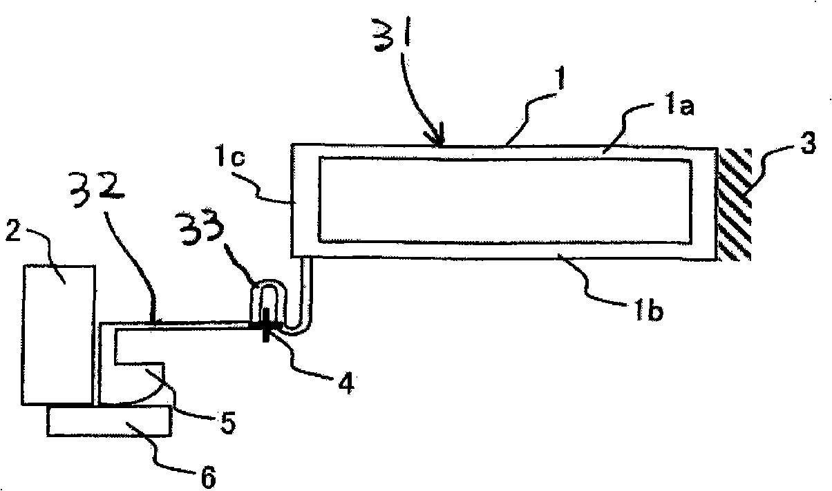
[0046] figure 1 The probe on the top is connected by parallel reeds 1, and its top and bottom sides form parallel beam parts 1a, 1b; on the other hand, the top part forms a vertical probe part 1c, and the base end constitutes a fixed The z deformation part 31 of the end 3; from the vertical probe part 1c of the parallel reed 1, extend the support arm 32, and set the top contact member 5 at the top end; the support arm 32 extends forward from the vertical probe part 1c , while setting the displacement absorbing part 33 in the central part; figure 1 In the illustration, the displacement absorbing part 33 is in reverse u-shape (u-shape is also possible), when the top contact member 5 is displaced (moved) in the up and down direction, in order to allow the top contact member ...

Embodiment 2

[0060] Image 6 and Figure 7 It is an illustration of the assembly of the probes related to the second embodiment of the present invention; Figure 8 It is an action description diagram of this implementation type; Image 6 It shows that the contact surface between the top contact members 5 is provided with a cleaning sheet (Cleaning Sheet) 7 made of a rough surface 7a; the structure of the cleaning sheet (Cleaning Sheet) 7 is for example Figure 7 As shown, a gap through which the probe can pass is provided on the resin sheet, and a cleaning sheet (Cleaning Sheet) 71 is provided on the single beam at the side of the gap, and the contact surface of the top contact member 5 can be coated with Microparticles such as cloth diamonds are realized; in addition, with the top of the rough surface 7a, the top contact member 5 of the contact part, after the cleaning sheet (Cleaning Sheet) 7 is set, through the relative offset, the rotation of the top contact member is accompanied by ...

Embodiment 3

[0065] Figure 9 It is an explanatory diagram of the tip contact member of the probe related to the third embodiment of the present invention; the shape of the tip contact member shown in Embodiments 1 and 2 can also be used such as Figure 8 The zigzag shape shown in the figure is used to promote the destruction of the oxide film, and through the rigid design and combination of the top contact components, a more suitable friction amount can be set.


PUM


Abstract

A probe which is cleaning-free, of which rubbing operation can be precisely controlled, and can be used for narrow-pitch pads, is provided. The probe assembly includes: a Z-deforming portion elastically deformable at least in a vertical direction; a tip contact element which includes a contact portion having a curved section, the tip contact element being connected to and supported on an end of the Z-deforming portion via an arm member, the contact portion being made to contact with an electrode pad and is vertically displaceable and rotatable; and a stopper for restricting movement of the tip contact element. After the tip contact element is rotated, due to pushing force from the electrode pad, for a certain distance in a direction of rotation, the stopper controls the movement of the tip contact element to prevent further rotation and to allow vertical movement.

Description

technical field [0001] The present invention relates to a kind of probe assembly, especially to a kind of probe (also known as measuring point assembly) used to form several chip circuit inspections on the wafer in the electronic equipment manufacturing process such as LSI (also called measuring point assembly), for example, Let the point-measuring probes in the wafer state contact the electrode blocks arranged on the chip so as to conduct electrical conduction on the chip at one time, and then assemble the probes built into the probe card for inspection of the circuit formed on the wafer. Background technique [0002] Improve the integration of electronic equipment accompanied by the progress of semiconductor technology, and on each chip formed on the wafer, the electrode blocks on the wafer chip will also be increased, and then through the reduction of the electrode block area and the distance between the electrode blocks Miniaturization, etc., in order to miniaturize the ...

Claims


Application Information

Patent Timeline
Patent Type & Authority Applications(China)
IPC IPC(8): G01R1/073G01R31/28
CPCG01R1/06716G01R1/06727G01R1/06738G01R1/073
Inventor 木本军生佐久间健
Owner 木本军生
Why Eureka
Try Eureka