Phase change storage unit using Schottky base diode as selection tube and its making method

A Schottky diode and phase-change memory technology, which is applied in the field of phase-change memory in microelectronics technology, can solve problems such as interference with adjacent unit read and write operations, achieve low power consumption, improve stability and consistency, and drive current Effect

Inactive Publication Date: 2008-09-10
SHANGHAI INST OF MICROSYSTEM & INFORMATION TECH CHINESE ACAD OF SCI
View PDF1 Cites 22 Cited by
  • Summary
  • Abstract
  • Description
  • Claims
  • Application Information

AI Technical Summary

Problems solved by technology

However, this technology also encounters some problems at present. For example, the diode prepared by this method will produce parasitic triodes, which will interfere with the read and write operations of adjacent cells [J.H.Oh, J.H.Park, Y.S. H.S.Lim, Y.T.Oh, J.S.Kim, J.M.Shin, J.H.Park, Y.J.Song, K.C.Ryoo, D.W.Lim, S.S.Park, J.I.Kim, J.H.Kim, J.Yu, F.Yeung, C.W.Jeong, J.H.Kong, D.H.Kang, G.H.Koh, G.T.Jeong, H.S.Jeong, and Kinam Kim; Full Integration of Highly Manufacturable 512MbPRAM based on 90nm Technology; Electron Devices Meeting, 2006.IEDM′06.International, 11-13Dec.2006Page(s):1-4]

Method used


Image

  • Phase change storage unit using Schottky base diode as selection tube and its making method
  • Phase change storage unit using Schottky base diode as selection tube and its making method
  • Phase change storage unit using Schottky base diode as selection tube and its making method

Examples


Embodiment Construction

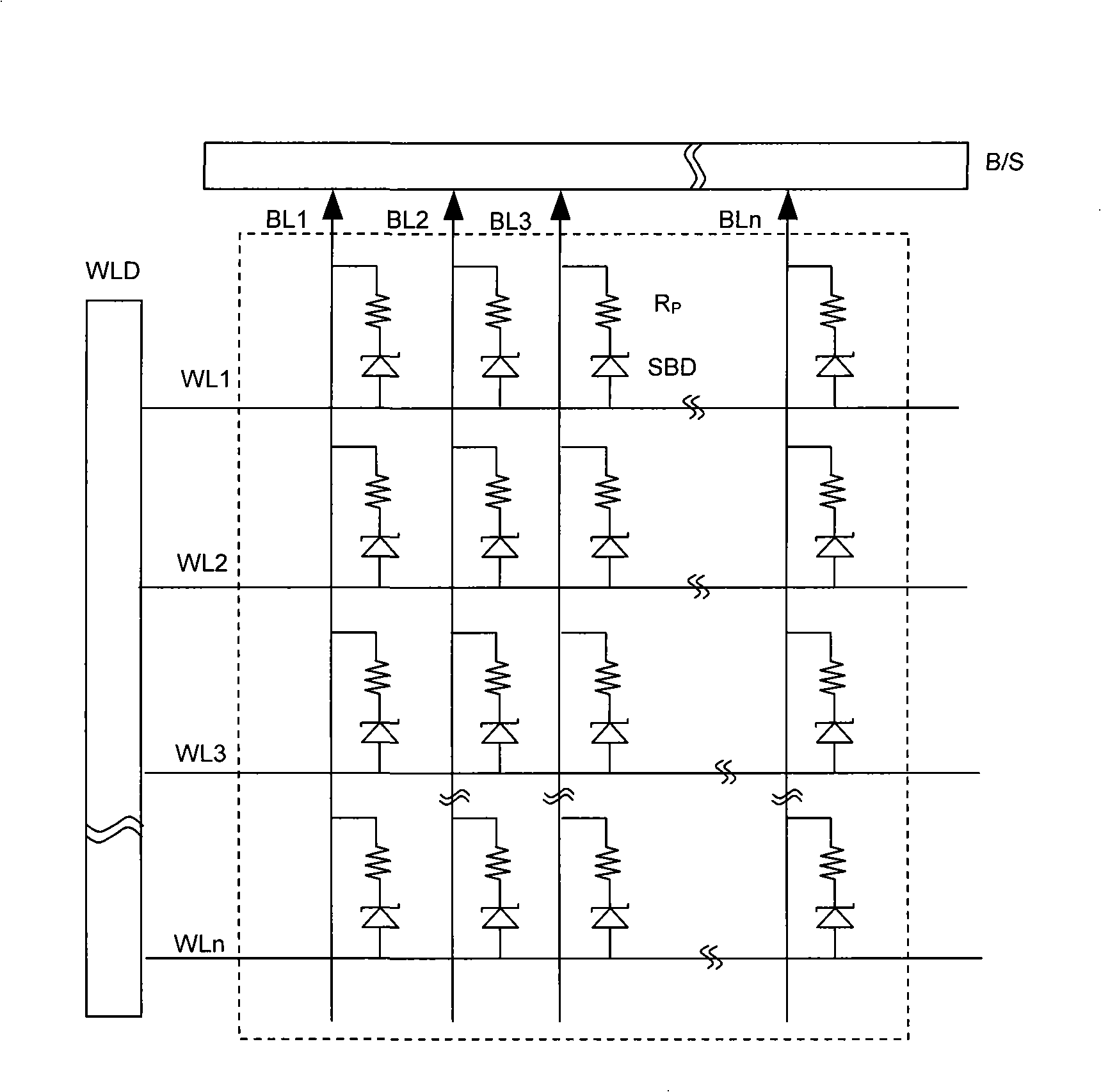
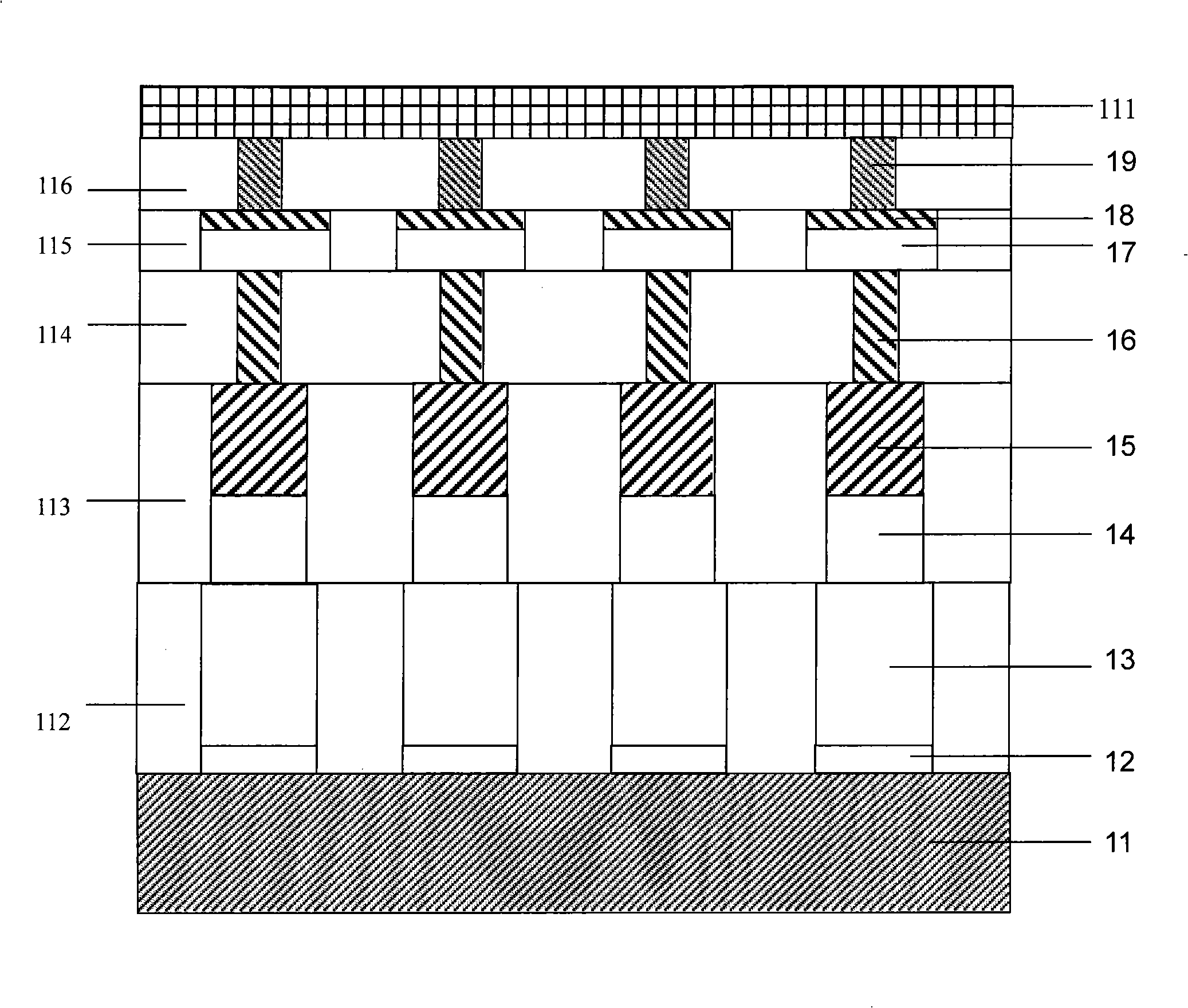
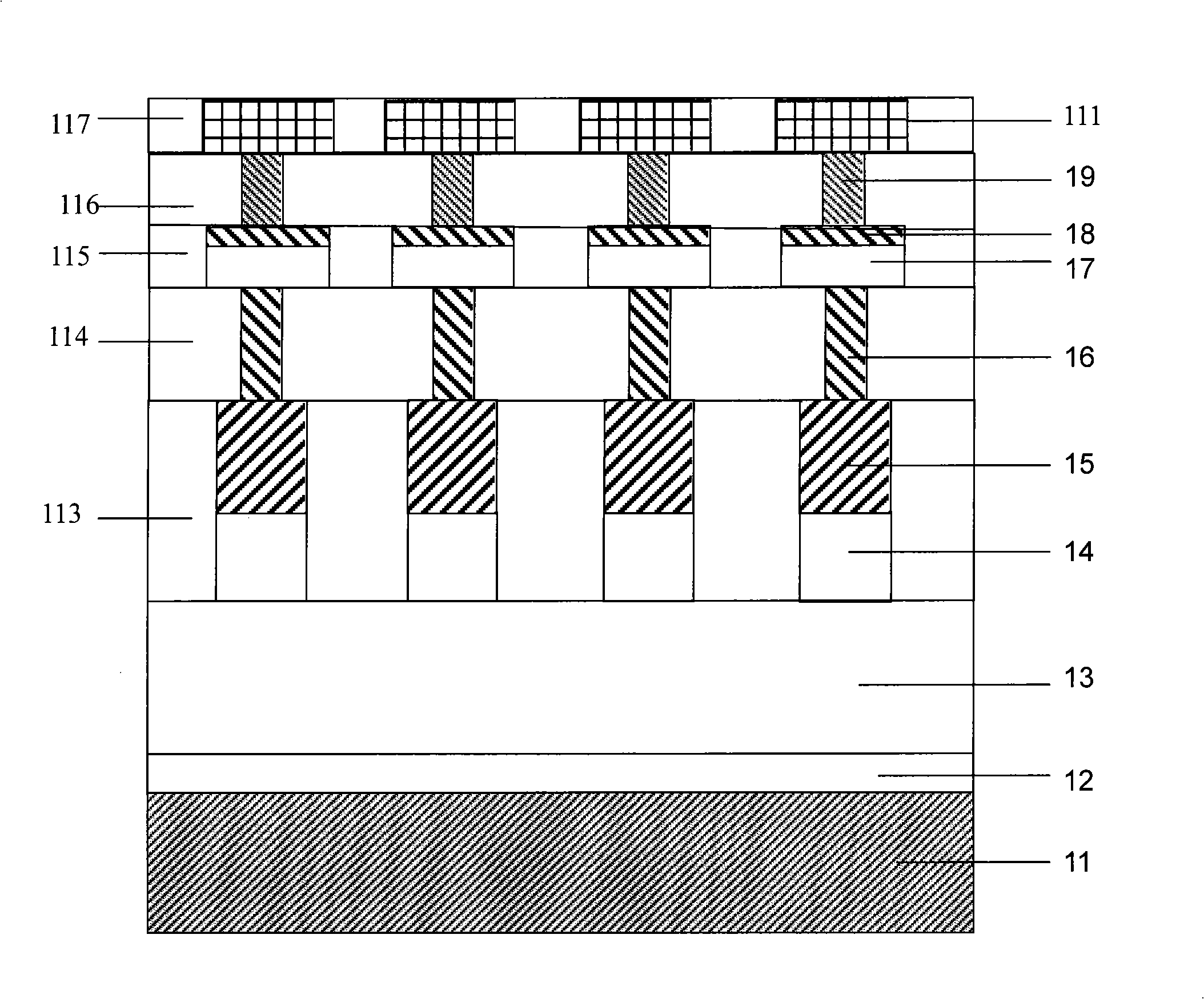
[0025] The invention is described more fully below with reference to the drawings, which provide preferred embodiments but should not be considered limited to the embodiments set forth herein. In the drawings, the thicknesses of layers and regions are appropriately exaggerated for clarity, but as schematic diagrams, they should not be considered to strictly reflect the proportional relationship of geometric dimensions. Here, the referenced figures are schematic diagrams of the present invention, and the representations in the figures are only schematic in nature and should not be considered as limiting the scope of the present invention.

[0026] Figure 2 to Figure 9 Methods of preparation of the examples of the invention are given. The following is a further introduction to the operation steps of preparing this ring-shaped phase-change memory unit in combination with the diagrams:

[0027] 1. If figure 2 As shown, an insulating dielectric layer 112 is deposited on the su...


PUM


Abstract

The invention pertains to the technical field of micro-electronics and discloses a phase change memory device provided with a Schottky diode and a preparation method thereof. The phase change memory device is basically characterized in that a structural unit is composed of the Schottky diode and the phase change memory device; the Schottky diode serves as a gate tube of the phase change memory device; the Schottky diode produces an N-type or P-type Si single crystal film by solid epitaxial technique and the N-type or P-type single crystal film forms a metal semiconductor contact together with a metal film. The Schottky diode prepared by the method has the advantages of stable performance, fast speed and great drive current. The structure disclosed by the invention is characterized in that the structure is applied to highly intense phase change memory devices and can lower the production cost of the phase change memory devices at the same time.

Description

technical field [0001] The invention relates to a phase-change storage unit using Schottky diodes and a preparation method, belonging to the field of phase-change storage in microelectronic technology. Background technique [0002] Memory occupies an important position in the semiconductor market. Only DRAM (Dynamnic Random Access Memory) and FLASH occupy 15% of the entire market. With the gradual popularization of portable electronic devices, the market for non-volatile memory is also growing. At present, FLASH It accounts for the mainstream of non-volatile memory, accounting for about 90%. However, with the advancement of semiconductor technology, FLASH has encountered more and more technical bottlenecks. First, the floating gate for storing charges cannot be thinned indefinitely with the development of integrated circuit technology. In addition, other shortcomings of FLASH technology also limit Its application, such as data writing is slow, high voltage is required when ...

Claims


Application Information

Patent Timeline
Patent Type & Authority Applications(China)
IPC IPC(8): H01L27/24H01L23/522H01L21/822H01L21/768G11C11/56G11C16/02
Inventor 凌云宋志棠封松林
Owner SHANGHAI INST OF MICROSYSTEM & INFORMATION TECH CHINESE ACAD OF SCI
Why Eureka
Try Eureka