

Method for manufacturing hundred nano-scale electric solenoid or net-shaped structure
A network structure and solenoid technology, applied in the fields of nanostructure manufacturing, nanotechnology, nanotechnology, etc., can solve the complex production process, no 100-nanometer solenoid or network structure, and many process steps, etc. problem, to achieve the effect of fewer process steps
- Summary
- Abstract
- Description
- Claims
- Application Information
AI Technical Summary
Problems solved by technology
Method used
Image

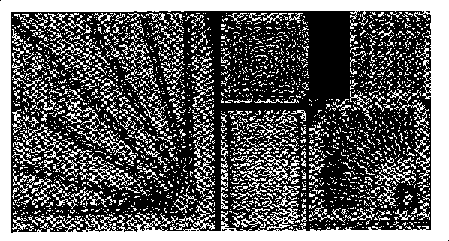
Examples
Embodiment
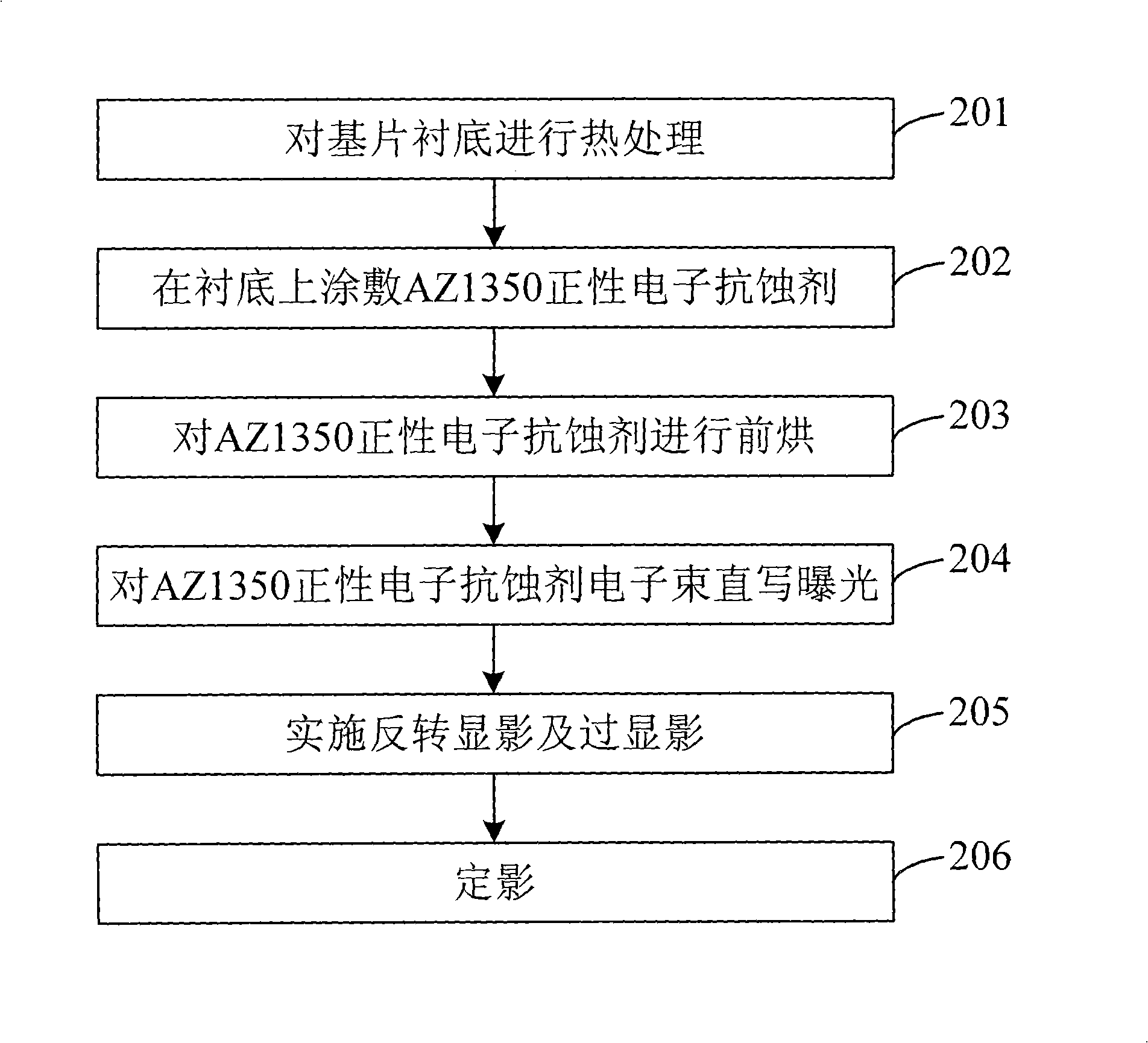
[0048] In this embodiment, taking AZ1350 positive electronic resist as an example, the detailed method and steps for fabricating a 100nm-scale solenoid or network structure by electron beam direct writing exposure technology are further described with reference to the accompanying drawings.
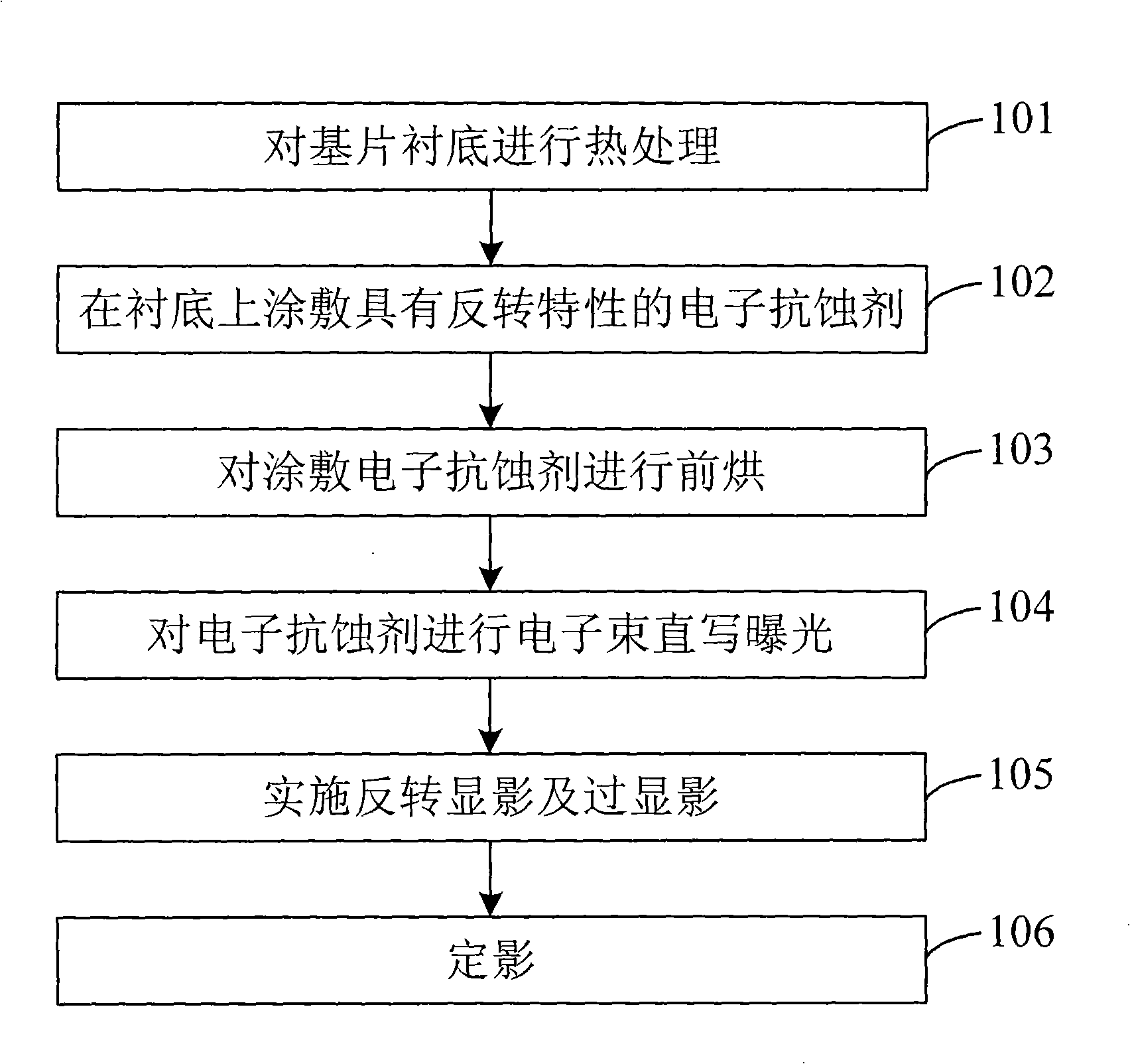
[0049] Such as figure 2 as shown, figure 2 It is a flow chart of a method for fabricating a hundred-nanometer-scale solenoid or a mesh structure using electron beam direct writing exposure technology according to an embodiment of the present invention. The method includes the following steps:
[0050] Step 201: performing heat treatment on the substrate;
[0051] In this step, the heat treatment includes performing strict surface cleaning treatment on the base substrate and high temperature treatment on a hot plate at 120 degrees for 2 minutes.
[0052] Step 202: coating AZ1350 positive electronic resist on the substrate;
[0053] In this step, the substrate is a flat and clean Si su...
PUM
 Abstract
Description
Claims
Application Information