ACF paste device and flat panel display

A technology for pasting devices and substrates, which is applied in the directions of identifying devices, instruments, and assembling printed circuits with electrical components, which can solve the problems of large-scale devices and large space.

Inactive Publication Date: 2008-10-01
HITACHI HIGH-TECH CORP
View PDF1 Cites 20 Cited by
  • Summary
  • Abstract
  • Description
  • Claims
  • Application Information

AI Technical Summary

Problems solved by technology

If the board size is large, a correspondingly large space

Method used


Image

  • ACF paste device and flat panel display
  • ACF paste device and flat panel display
  • ACF paste device and flat panel display

Examples


Embodiment Construction

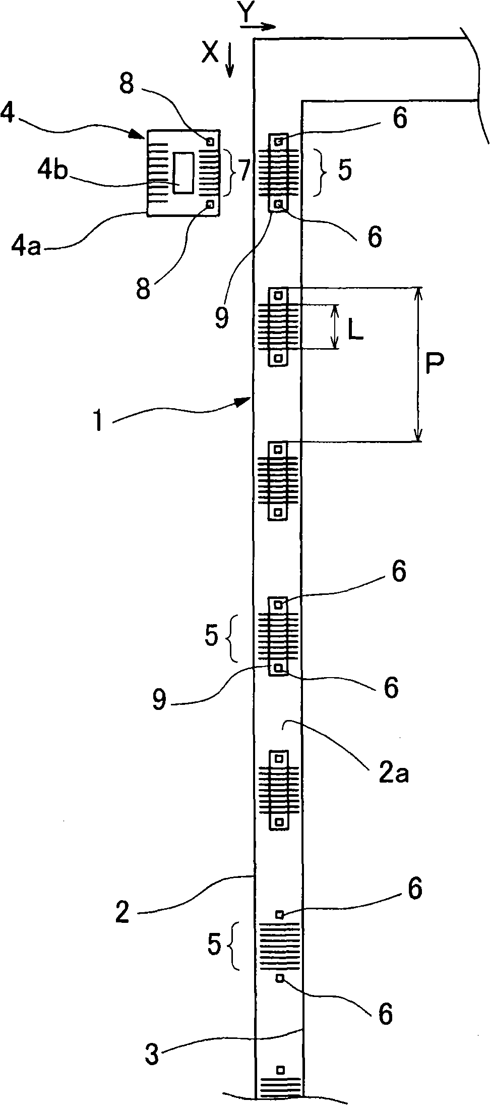
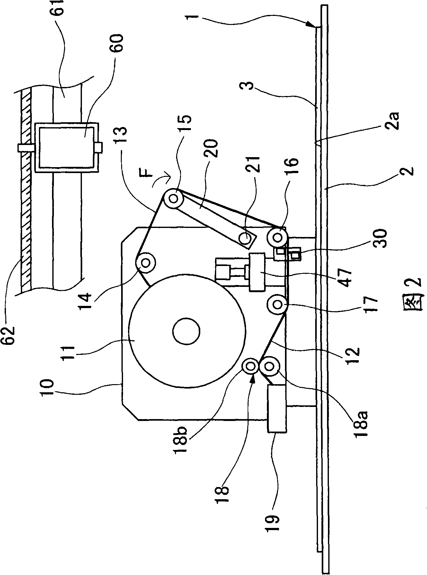
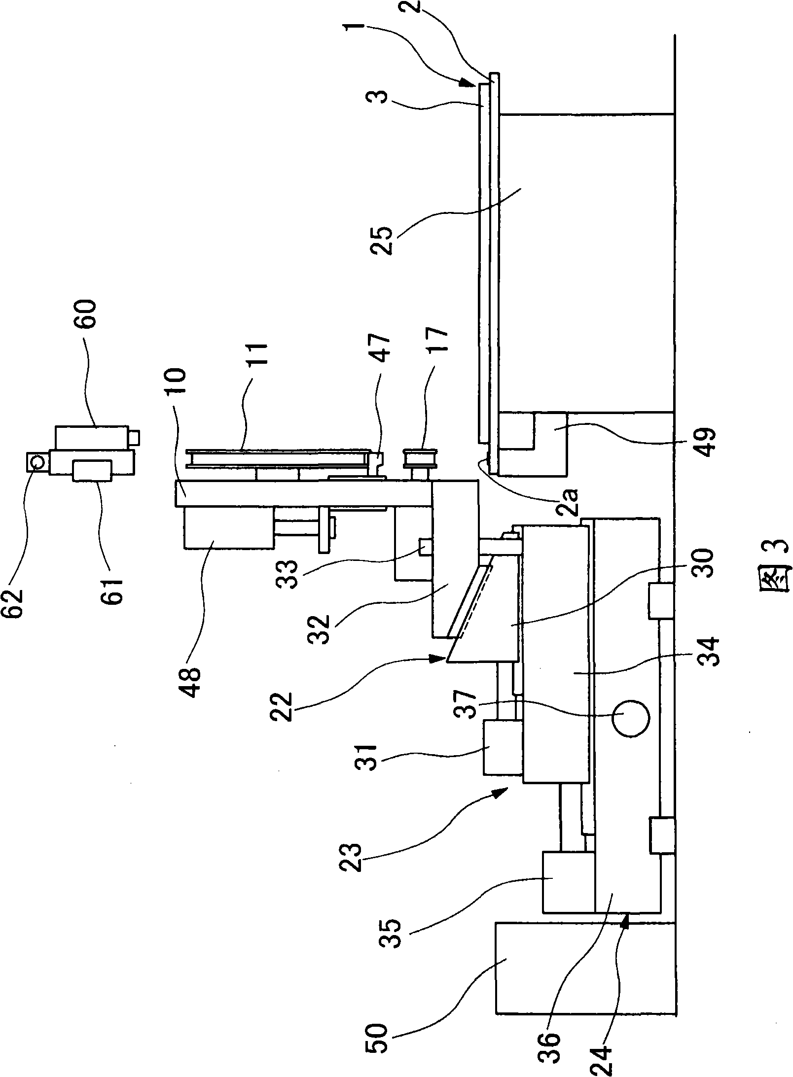
[0030] Hereinafter, embodiments of the present invention will be described with reference to the drawings. figure 1 A liquid crystal panel is shown as an example of a substrate on which ACF is pasted, and a drive circuit including TCP mounted on the substrate by TAB is shown as an example of a semiconductor circuit element mounted on the ACF. In addition, the substrate is not limited to a substrate constituting a liquid crystal panel, and may be a printed circuit board or the like, and what is mounted on the substrate is not limited to a drive circuit, and may be a circuit electrically connected through an ACF.

[0031] figure 1 Among them, 1 is a liquid crystal panel. The liquid crystal panel 1 is composed of a lower substrate 2 and an upper substrate 3. Both the lower substrate 2 and the upper substrate 3 are made of glass thin plates, and liquid crystal is sealed between the two substrates 2 and 3. The lower substrate 2 protrudes from the upper substrate 3 by a predetermin...


PUM


Abstract

A paste unit for pasting ACF (9) to the jut (2a) of the lower substrate (2) of the liquid crystal panel (1) is composed of a supply scroll (11) for supplying ACF adhesive tape (13), a cut-off unit (40) for the moving path of the ACF adhesive tape (13) supplied from the supply scroll (11), and a bonding head (47). The paste unit is installed on the bearing component (10), which is installed on the transport mechanism (36) driven by the guide screw (37), the liquid crystal panel (1) is loaded on the platform (25), so that the transport mechanism (36) is transported in the array direction of the electrode group (5) of the liquid crystal panel (1), the bearing component (10) installed with the paste unit is located in each interval of the paste part of the ACF (9), to paste the ACF (9).

Description

technical field [0001] The present invention relates to an ACF pasting device for pasting ACF (Anisotropic Conductive Film) on a substrate in order to mount a semiconductor circuit element such as a driver circuit on the substrate, and a flat panel display device including the ACF pasted by the ACF pasting device . The aforementioned substrate is constituted by a display panel constituting a flat panel display device such as a liquid crystal display or a plasma display. Background technique [0002] A liquid crystal display is constituted, for example, by connecting a printed circuit board via a semiconductor circuit element to a liquid crystal panel composed of two upper and lower transparent substrates in which a liquid crystal sealing space is formed. Here, the semiconductor circuit element is a drive circuit. The drive circuit has inner and outer electrodes, the inner electrode is electrically connected to one substrate constituting the liquid crystal panel, and the out...

Claims


Application Information

Patent Timeline
IPC IPC(8): H05K3/30H05K13/04G02F1/13G09F9/00
Inventor 斧城淳野本秀树平迫弘司峰川英明
Owner HITACHI HIGH-TECH CORP
Why Eureka
Try Eureka