Welding connection structure of terminal of electronic device and printed circuit board

A technology for printed circuit boards and electronic devices, which is applied in the field of soldered connection structures, can solve problems such as weakened installation strength, complicated assembly operations, and larger occupied area, and achieve the effect of improving installation strength

Inactive Publication Date: 2008-10-08
SMK CO LTD
View PDF2 Cites 7 Cited by
  • Summary
  • Abstract
  • Description
  • Claims
  • Application Information

AI Technical Summary

Problems solved by technology

[0006] However, in Figure 20 In the conventional example shown in FIG. 21, although the occupied area required for the solder connection on the printed circuit board 105 can be reduced, there is a change in the strength (mounting strength) of fixing the connector 103 on the printed circuit board 105. weak question
[0007] In addition, in Figure 22 In the existing example shown, there is also the same Figure 20 21, and since it is necessary to form a plurality of holes for inserting plug-in terminals 206 to 206 on the printed circuit board 202, the required circuit board occupation area becomes larger, and there is a problem that the printed circuit board 202 cannot be The other side of the side panel is used for circuit configuration issues
[0008] In addition, if the number of surface mount terminals 205 to 205 is increased in order to increase the mounting strength, there is a problem that the assembly work becomes complicated.
[0009] In addition, in Figure 20 21, it is also considered to form terminal insertion holes on the printed circuit board 105, insert the connection terminals of the connector 103 into the insertion holes, and solder the connection parts to the structure on the pad, but since the terminal insertion holes are required Therefore, there is a problem that the occupied area required for the solder connection on the printed circuit board becomes large, and the board surface on the opposite side to the connector mounting surface of the printed circuit board cannot be used for circuit configuration.

Method used


Image

  • Welding connection structure of terminal of electronic device and printed circuit board
  • Welding connection structure of terminal of electronic device and printed circuit board
  • Welding connection structure of terminal of electronic device and printed circuit board

Examples


Embodiment Construction

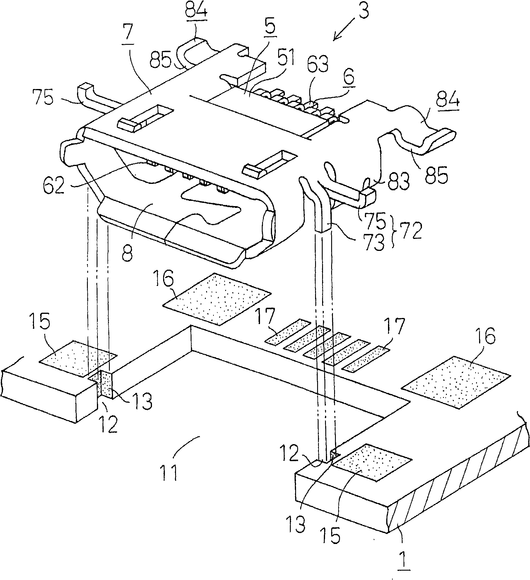
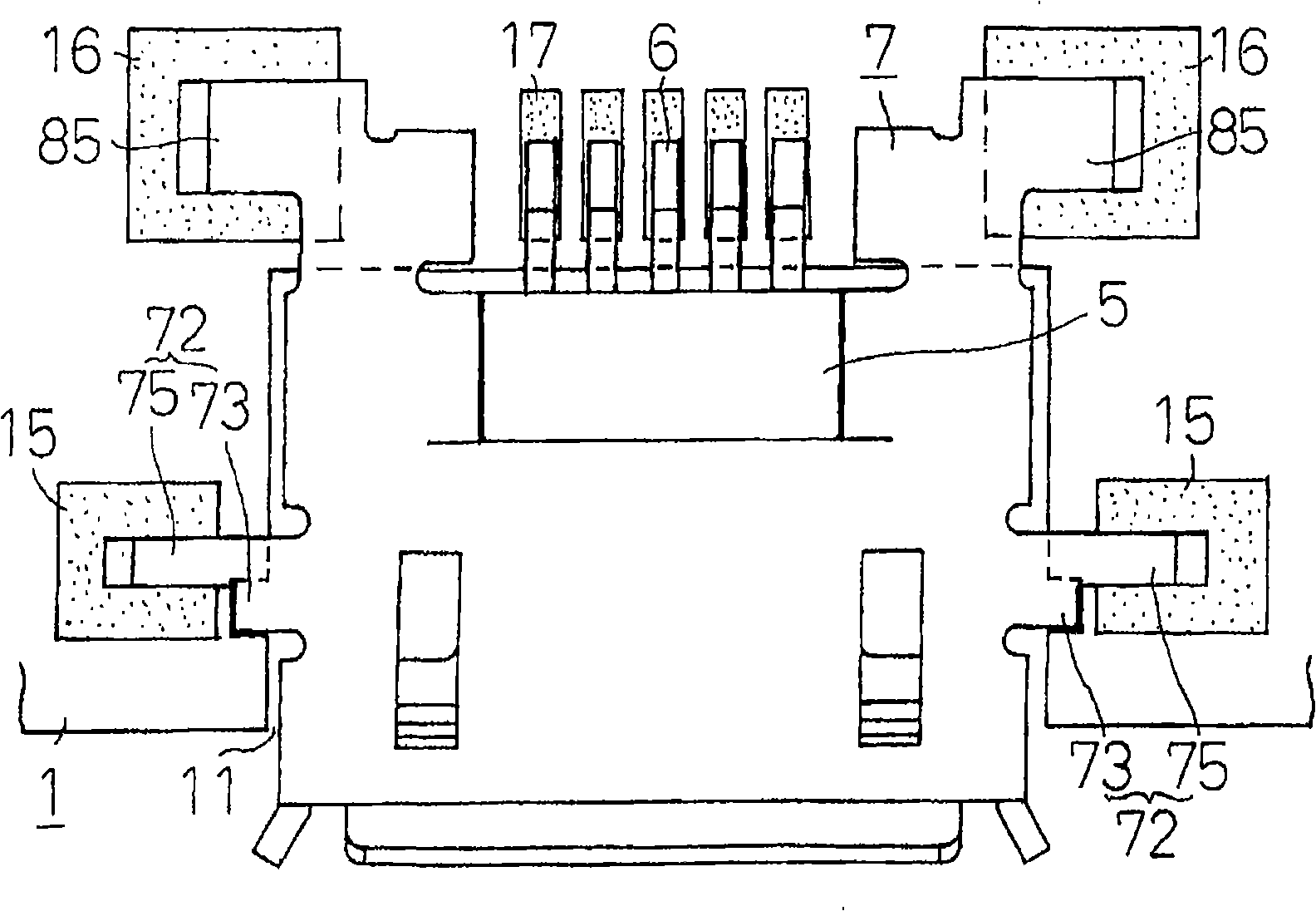
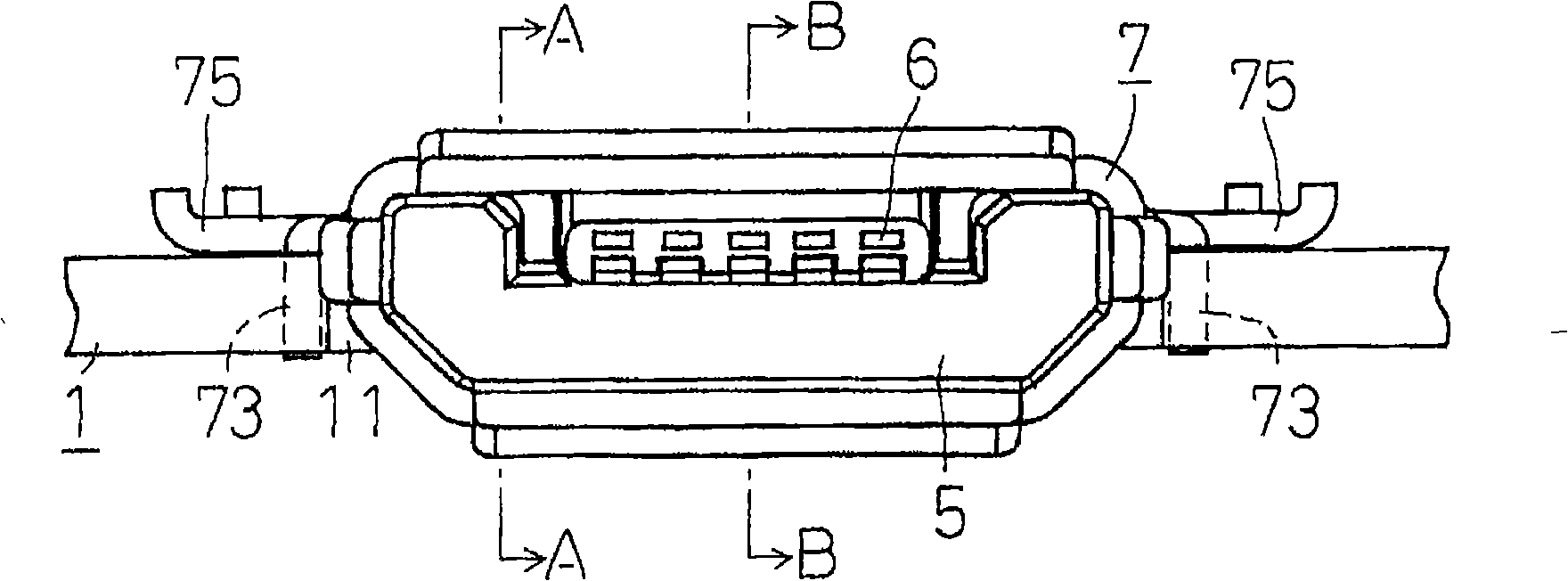
[0045] Figure 1 to Figure 7 It is a figure showing one embodiment of the solder connection structure between the terminal of the electronic device and the printed circuit board of the present invention. In these figures, 1 is a printed circuit board, and 3 is a socket (small USB connector) as an example of an electronic device. one example).

[0046] Formed on the edge of the printed circuit board 1 as figure 1 and figure 2 Shown cutout 11, is formed with small cutout 12,12 in the relative left and right sides of this cutout 11, on the side face of this cutout 12,12, is formed with the first soldering pad (for example by the copper that forms by electroplating) that connects. foil) 13,13.

[0047]Second pads (such as copper foil) 15, 15 for soldering connection are formed on the left and right edges of the slit 11, and a third pad (such as copper foil) for soldering connection is formed on the edge of the back side of the slit 11. 16, 16 and fourth pads (such as copper ...


PUM


Abstract

The present invention provides a welding connection structure between a terminal of a electron device with improving mounting strength of a plug (3) on a printed circuit board (1) and a printed circuit board without increasing welding area of a circuit board. Matching the plug (3) at an incision (11) at the edge of the printed circuit board (1), and welding a connecting terminal (72, 72) of a shielding cover of the plug (3) on a solder pad of the printed circuit board (1), forming first and second solder pad (13, 13, 15, 15) at side and edge of the incision (11), the connecting terminal (72, 72) provided with first and second connector (73, 73, 75, 75) of the plug welding connecting with the first and second solder pad (13, 13, 15, 15) toward the incision (11).

Description

technical field [0001] The present invention relates to a solder connection structure of a terminal of an electronic device (such as a connector) and a printed circuit board having a cutout or a through hole for fitting the electronic device. [0002] In particular, it relates to a solder connection structure between a terminal and a printed circuit board suitable for mounting small electronic devices such as small SUB connectors for mobile phones and personal computers on a printed circuit board. Background technique [0003] In the past, in the solder connection structure of such a terminal and a printed circuit board, there is known a structure in which in order to suppress the protruding height from the surface of the printed circuit board and realize thinning and miniaturization, A cutout or through-hole structure that can fit electronic devices is provided. (For example, refer to Patent Document 1: JP-A-2000-133391 or Patent Document 2: JP-A-2004-79407). [0004] In ...

Claims


Application Information

Patent Timeline
Patent Type & Authority Applications(China)
IPC IPC(8): H05K3/34H01R4/02
Inventor 鸨田润一
Owner SMK CO LTD
Why Eureka
Try Eureka