

Three-dimensionally integrated semicondutor device and method for manufacturing the same
a semiconductor and three-dimensional technology, applied in semiconductor devices, semiconductor/solid-state device details, electrical apparatus, etc., can solve the problems of complex structure of devices, difficulty in forming large amounts of wiring on the post electrode side, and need similar facilities, so as to improve the performance of rf (radio frequency) modules, improve high-frequency characteristics, and reduce the installation area.
- Summary
- Abstract
- Description
- Claims
- Application Information
AI Technical Summary
Benefits of technology
Problems solved by technology
Method used
Image

Examples
first embodiment
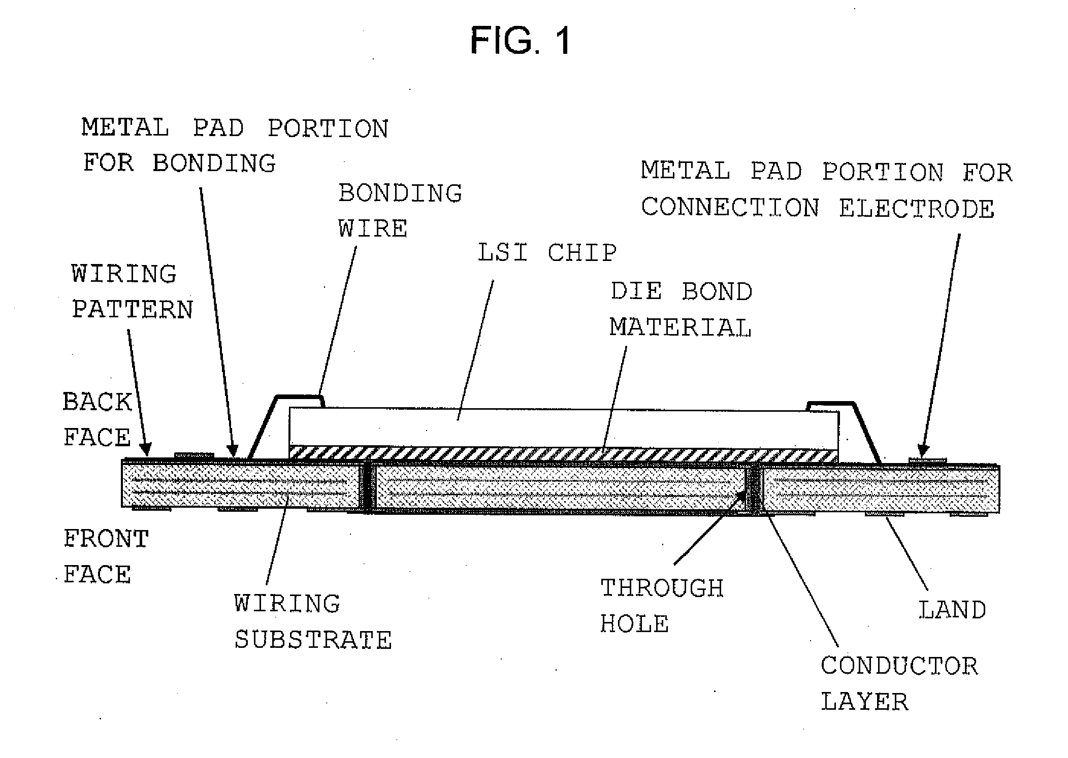
[0036]The present invention will now be described by way of example. the three-dimensionally integrated semiconductor device of the present invention will be described with reference to FIGS. 1 to 8. FIG. 1 is a view showing a state in which a semiconductor chip (LSI chip) is bonded and connected to the back face of a wiring substrate (multilayer organic substrate). Notably, in the following description, the upper side of the wiring substrate in FIG. 1 on which the LSI chip is mounted will be referred to as the back face (first main face), and the lower side of the wiring substrate in FIG. 1 on which another circuit element is mounted as will be described later will be referred to as the front face (second main face). In the illustrated example, the LSI chip is bonded to the upper side (as viewed in FIG. 1) of the multilayer organic substrate by use of a die bond material, and is connected to the uppermost wiring pattern of the organic substrate via bonding wires. Metal pad portions...
second embodiment
[0053]FIG. 11 is a plan view showing an example in which the semiconductor device of the second embodiment is used. FIG. 12 is a side cross-sectional view showing one of semiconductor modules A to C shown in FIG. 11. As shown in FIGS. 11 and 12, the semiconductor modules A to C and circuit elements such as capacitors are disposed on the wiring pattern of the mother substrate, and are electrically and mechanically connected thereto by means of soldering or the like. At that time, as shown in FIG. 12, solder fillets (the shape of solder surface formed at a connection portion after solidification of solder) are formed such that meniscuses (the shape formed by the surface of liquid when the surface deforms into a curved shape due to force such as surface tension) are formed on the side surfaces of the post electrodes exposed to the side surfaces of the resin seal, whereby connection strength can be increased.
[0054]Next, a third embodiment of the present invention will be described with ...
fifth embodiment
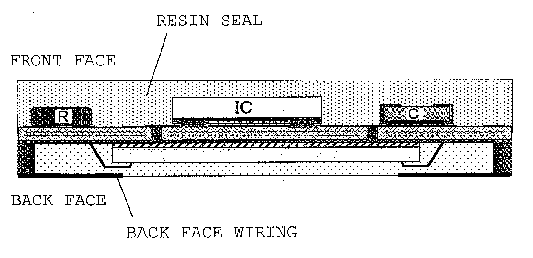
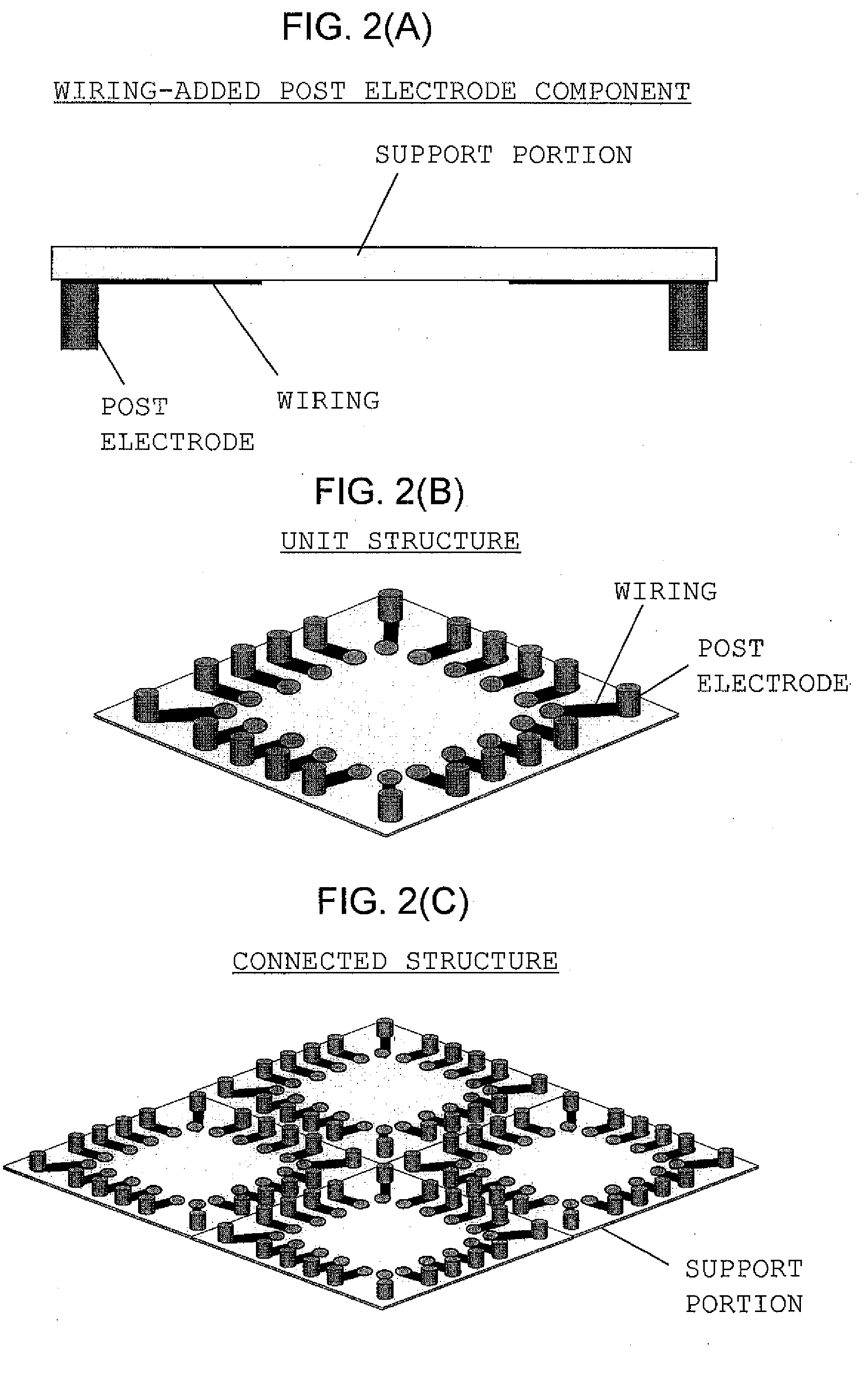
[0056]FIG. 17 is a view for describing the present invention. After the circuit element IC is attached to the front face of the wiring substrate (organic substrate) as shown in FIG. 13, as in the case of the back face side, a wiring-added post electrode component as shown in FIGS. 2(A) to 2(C) is attached to the front face side. After that, as in the above-described example, the front face side is resin-sealed, and the support plate is separated. After that, various circuit elements (resistances R and capacitors C) are flip-chip-bond-connected to the front face wiring traces. As a result, a semiconductor device in which circuit elements are stacked in three tiers can be fabricated. By means of stacking another wiring-added post electrode component, circuit elements can be connected in four or more tiers.
[0057]FIG. 18(A) is a perspective view showing a wiring-added post electrode component different from that shown in FIGS. 2(A) to 2(C), FIG. 18(B) is a cross-sectional view of the wi...
PUM
 Abstract
Description
Claims
Application Information