Optical module

a technology of optical modules and optical components, applied in the field of optical modules, can solve the problems of degrading high-frequency characteristics and high impedance, and achieve the effect of improving high-frequency characteristics and lowering the impedan

Pending Publication Date: 2022-09-22
CIG PHOTONICS JAPAN LTD
View PDF0 Cites 1 Cited by
  • Summary
  • Abstract
  • Description
  • Claims
  • Application Information

AI Technical Summary

Benefits of technology

[0007]The metallization pattern is on the surface of the dielectric block, whereby impedance can be lowered due to capacitance of the dielectric block. This can improve the high-frequency characteristics.

Problems solved by technology

This results in a higher impedance and degrades high-frequency characteristics.

Method used


Image

  • Optical module
  • Optical module
  • Optical module

Examples


first embodiment

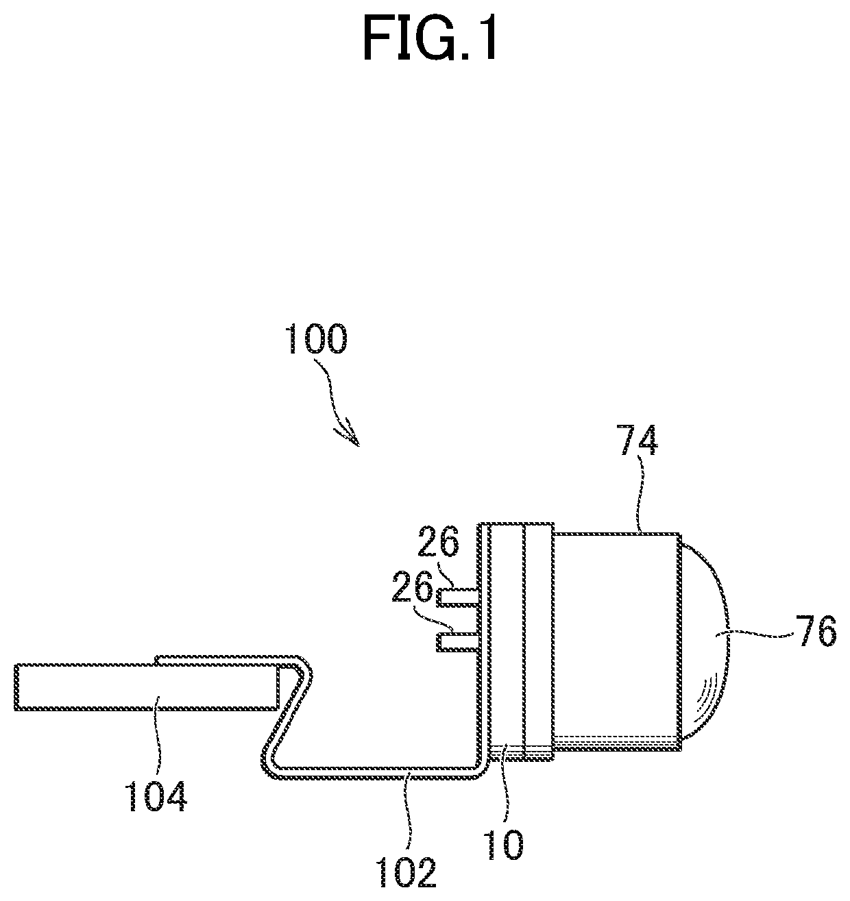
[0016]FIG. 1 is a side view of an optical module according to a first embodiment. An optical module 100 is a TO-CAN (Transistor Outline-Can) type optical module and may be any one of a transmitter optical sub-assembly (TOSA) equipped with a light emitting device, a receiver optical sub-assembly (ROSA) equipped with a light receiving device, and a bidirectional module (BOSA) equipped with both the light emitting device and the light receiving device. The optical module 100 has a flexible printed circuit board (FPC) 102, which is connected to a printed circuit board (PCB) 104. The optical module 100 has a conductive stem 10.

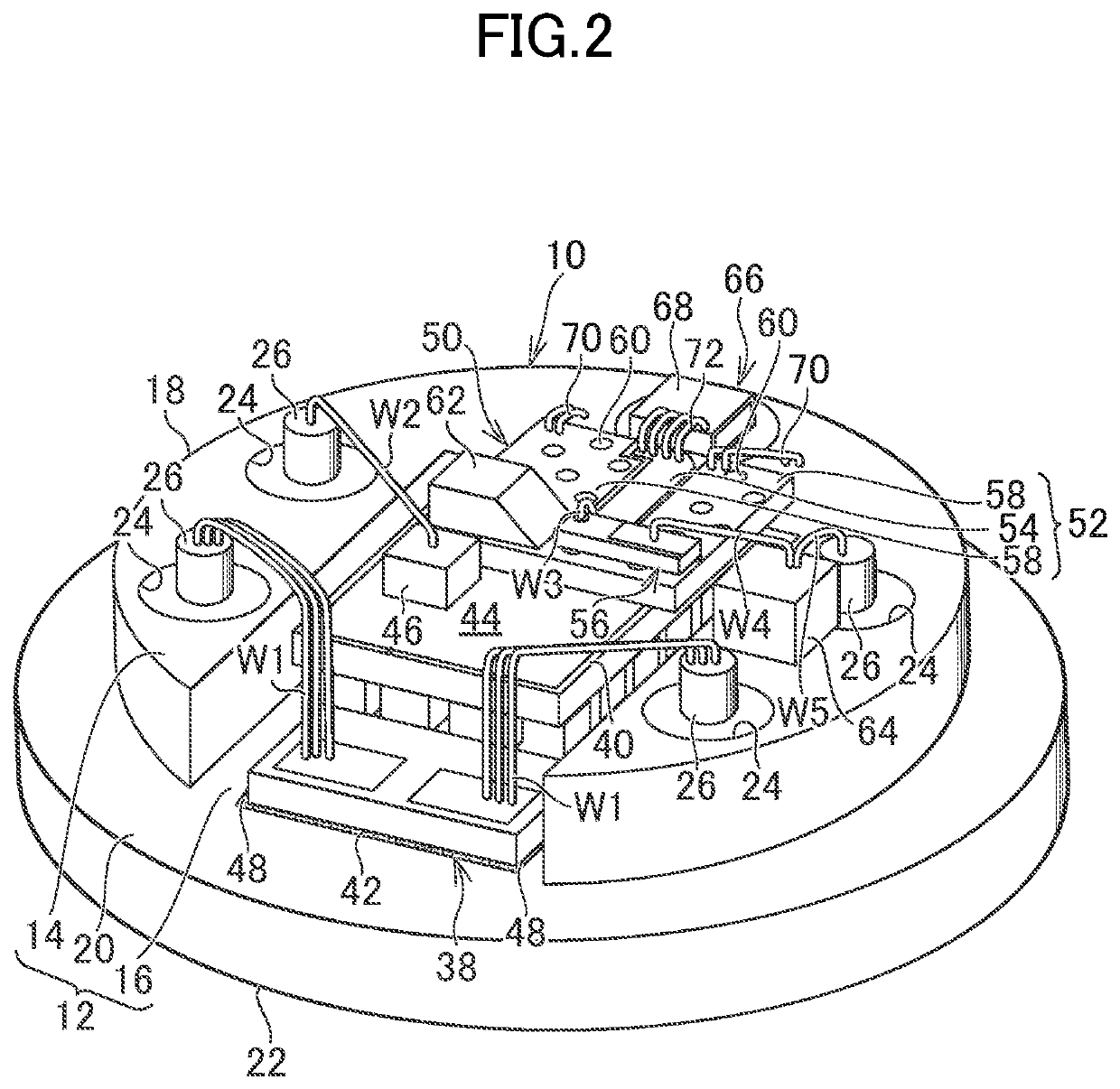
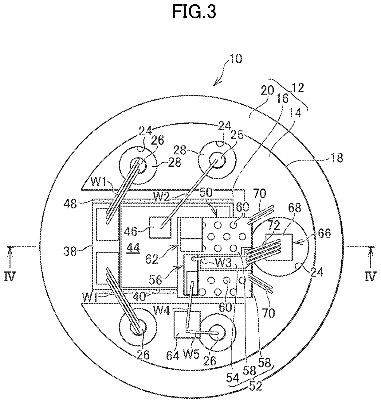
[0017]FIG. 2 is perspective view of a conductive stem 10 and electronic components mounted on it. FIG. 3 is a plan view of the conductive stem 10 and the electronic components mounted on it. FIG. 4 is a IV-IV cross-sectional view of a structure in FIG. 3.

[Conductive Stem]

[0018]The conductive stem 10 is made of a conductor such as metal. The conductive stem 10 is co...

second embodiment

[0038]FIG. 6 is a perspective view of a conductive stem and electronic components mounted on it according to a second embodiment.

[0039]The second dielectric block 266 has the second metallization pattern 268 on the surface. The second dielectric block 266 is mounted to the first surface 212 of the conductive stem 210. The second metallization pattern 268 is electrically continuous to the conductive stem 210. The ground wire 270 electrically connects the second metallization pattern 268 to the interconnection pattern 252 (ground pattern 258) of the sub-mount substrate 250. What is described in the first embodiment is applicable to other contents.

[0040]FIG. 7 is frequency characteristics of a comparative example, the first embodiment, and the second embodiment, calculated by a three-dimensional electromagnetic field simulator HFSS (High Frequency Structure Simulator). In the comparative example, the signal wire was bonded directly to the signal lead pin. It can be seen that the transm...


PUM

PropertyMeasurementUnit
conductiveaaaaaaaaaa
electricalaaaaaaaaaa
diameteraaaaaaaaaa

Abstract

An optical module includes: a conductive stem having first and second surfaces; some lead pins including a signal lead pin; a sub-mount substrate having an interconnection pattern; a photoelectric device mounted on the sub-mount substrate and electrically connected to the interconnection pattern; a dielectric block having a metallization pattern on a surface; and a signal wire electrically connecting the metallization pattern to the interconnection pattern. Each lead pin includes a shaft portion inside a corresponding one of the through holes, a first end portion projecting from the first surface, and a second end portion projecting from the second surface. The signal lead pin has the first end portion larger in diameter than the shaft portion. The dielectric block is opposed to and fixed to a tip face of the first end portion of the signal lead pin. The metallization pattern is electrically continuous to the tip face.

Description

CROSS-REFERENCE TO RELATED APPLICATION[0001]The present application claims priority from Japanese patent application JP2021-044440 filed on Mar. 18, 2021, the contents of which are hereby incorporated by reference into this application.BACKGROUND1. Field[0002]This disclosure relates to an optical module.2. Description of the Related Art[0003]Small optical modules are required to have improved high-frequency characteristics. A transistor outline can (TO-CAN) package (JP 2011-108939A) uses lead pins to transmit electrical signals to an edge emitting laser. Each lead pin penetrates a conductive stem with a dielectric interposed between them to form a coaxial line.[0004]Bonding wires are used to make electrical connections from the lead pins. A shorter bonding wire has its lower impedance, while the lead pin should protrude longer from the conductive stem to use the shorter bonding wire. This results in a higher impedance and degrades high-frequency characteristics.SUMMARY[0005]This dis...

Claims


Application Information

Patent Timeline
Patent Type & Authority Applications(United States)
IPC IPC(8): H01S5/0232H01S5/02253H01S5/02255
CPCH01S5/0232H01S5/02253H01S5/02255H01S5/02212H01S5/02326H01S5/02345H01S5/0237H01S5/0239H01S5/02415H01S5/0262H01S5/06226H01S5/0265
Inventor NOGUCHI, DAISUKEYAMAMOTO, HIROSHI
Owner CIG PHOTONICS JAPAN LTD
Why Eureka
Try Eureka