

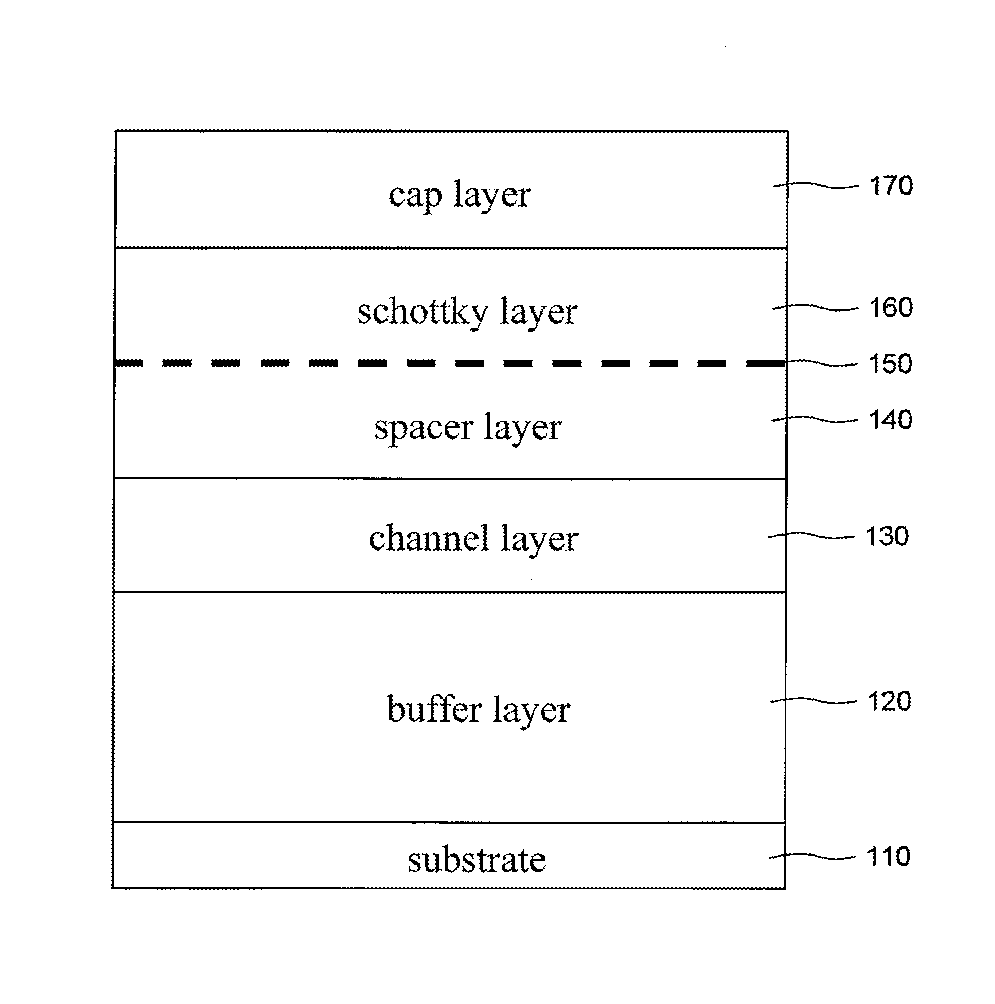
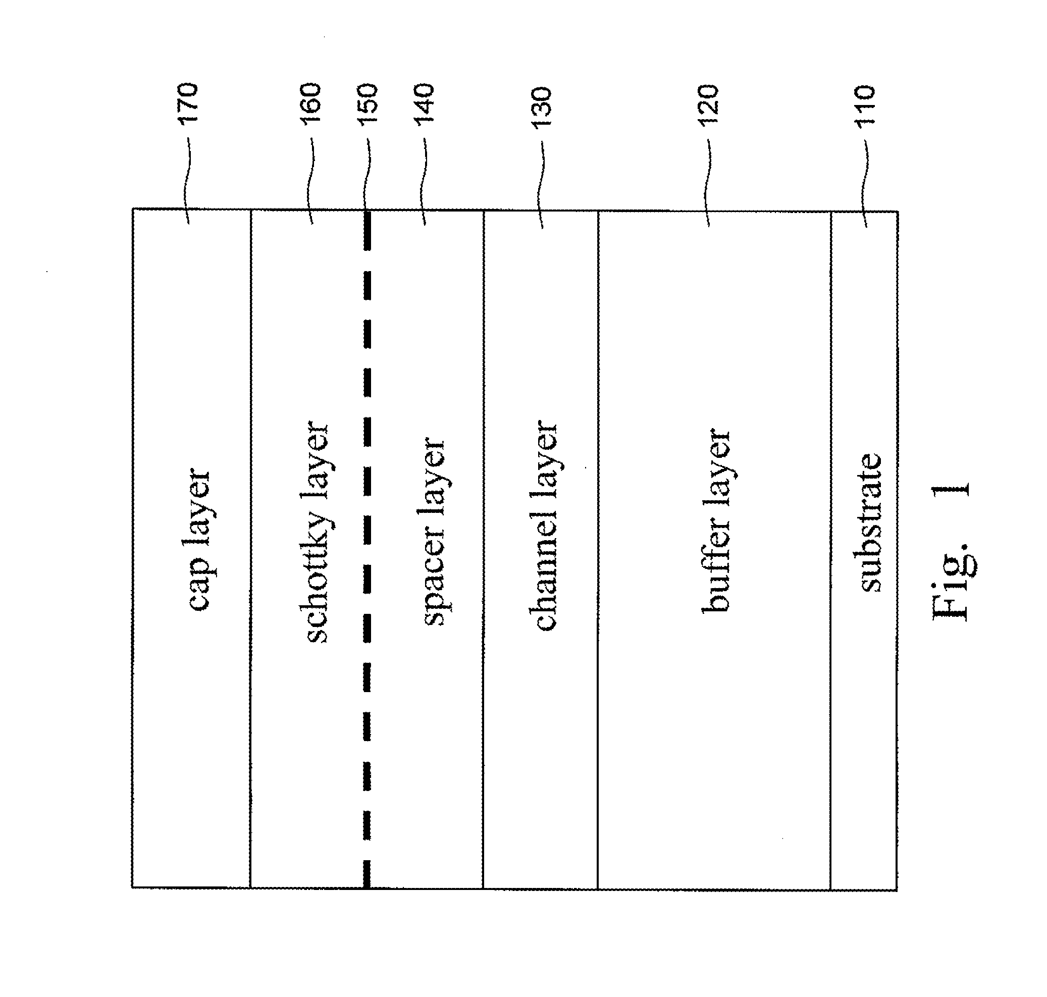
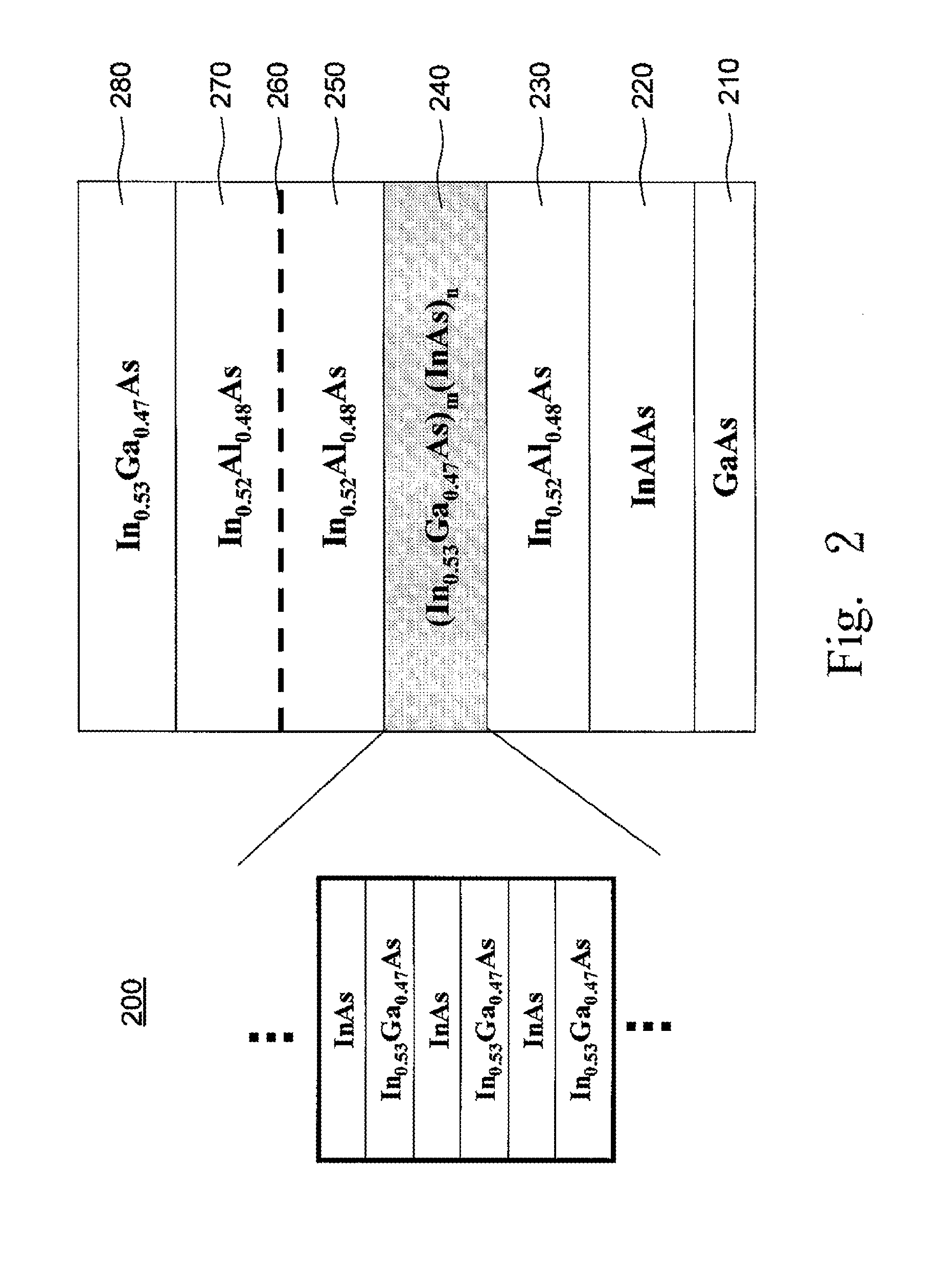
High Electron Mobility Transistor and Method for Fabricating the Same
a high-electromagnetic transistor and electron mobility technology, applied in the field of high-frequency devices, can solve the problems of insufficient effective mass, difficult epitaxy growth, complex composition of superlattice structure,
- Summary
- Abstract
- Description
- Claims
- Application Information
AI Technical Summary
Benefits of technology
Problems solved by technology
Method used
Image

Examples
Embodiment Construction
[0020]In the following description, several specific details are presented to provide a thorough understanding of the embodiments of the present invention. One skilled in the relevant art will recognize, however, that the present invention can be practiced without one or more of the specific details, or in combination with or with other components, etc. In other instances, well-known implementations or operations are not shown or described in detail to avoid obscuring aspects of various embodiments of the present invention.
[0021]The terms used in this specification generally have their ordinary meanings in the art and in the specific context where each term is used. The use of examples anywhere in this specification, including examples of any terms discussed herein, is illustrative only, and in no way limits the scope and meaning of the invention or of any exemplified term. Likewise, the present invention is not limited to various embodiments given in this specification.
[0022]As use...
PUM
 Abstract
Description
Claims
Application Information