Pixel array substrate and LCD device
A technology for pixel array substrates and liquid crystal display devices, which can be used in static indicators, nonlinear optics, instruments, etc., and can solve problems such as flickering or unevenness of the screen, difficult control of pixel patterning process, and inability to accurately compensate
- Summary
- Abstract
- Description
- Claims
- Application Information
AI Technical Summary
Problems solved by technology
Method used
Image

Examples
Embodiment Construction
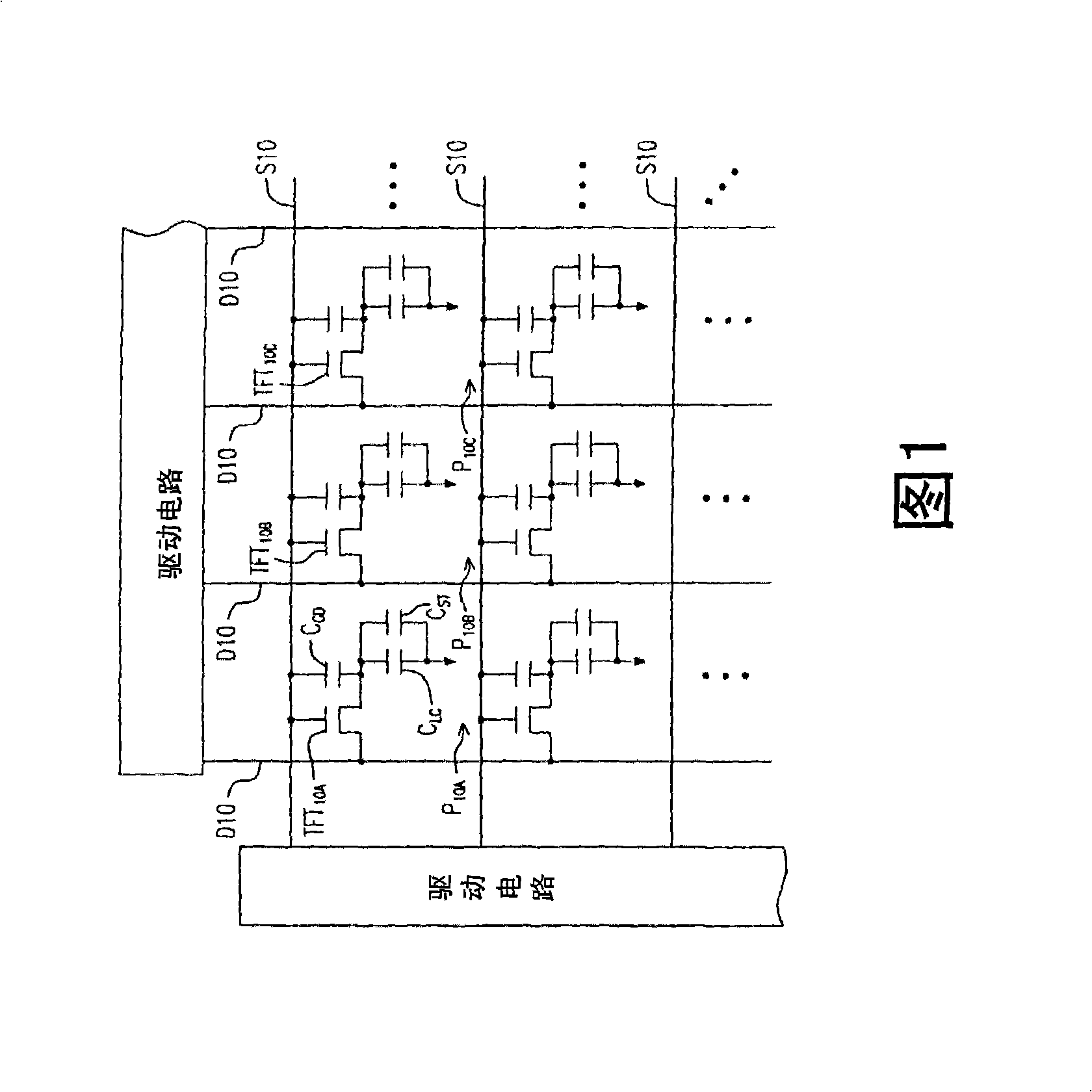
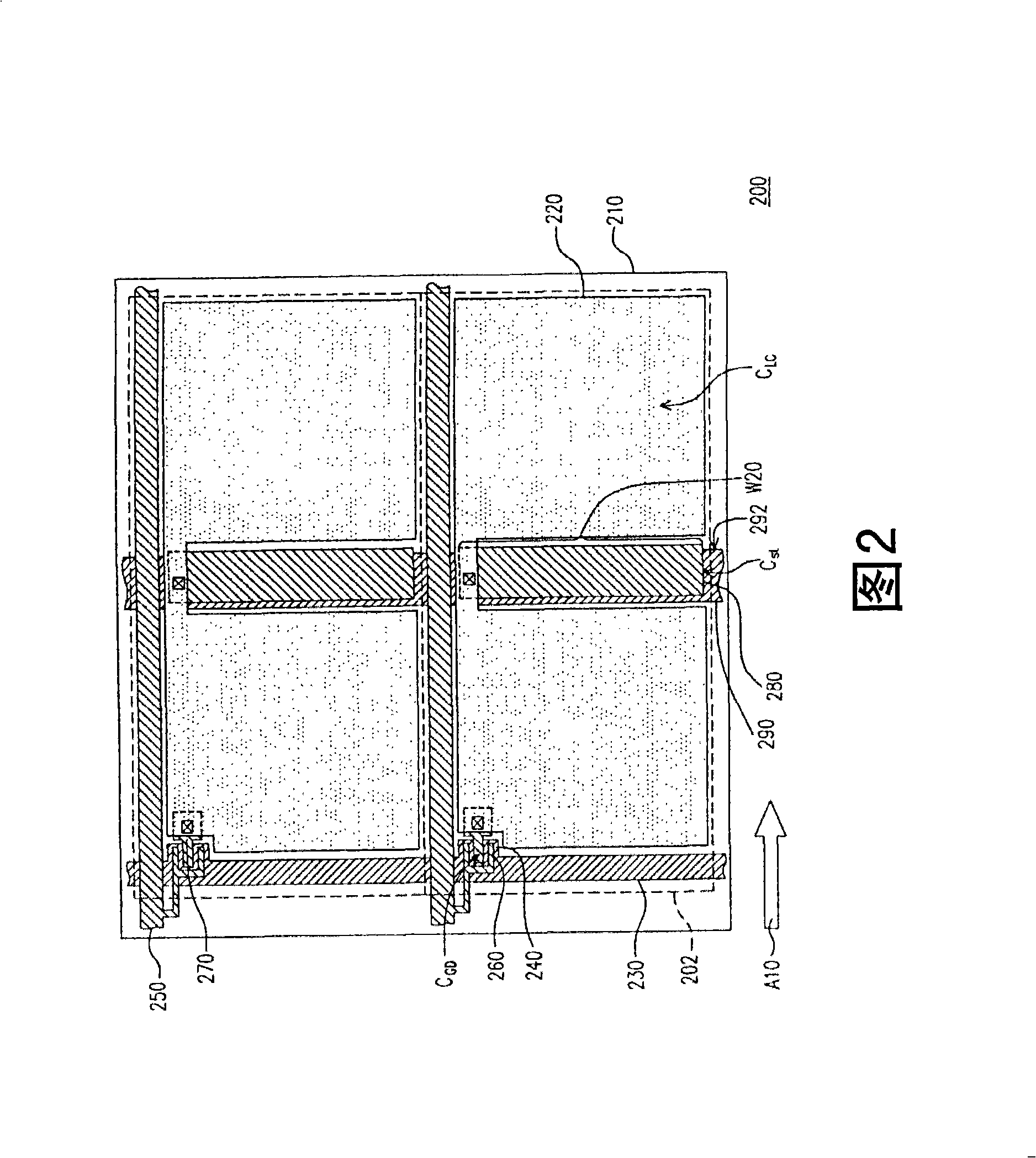
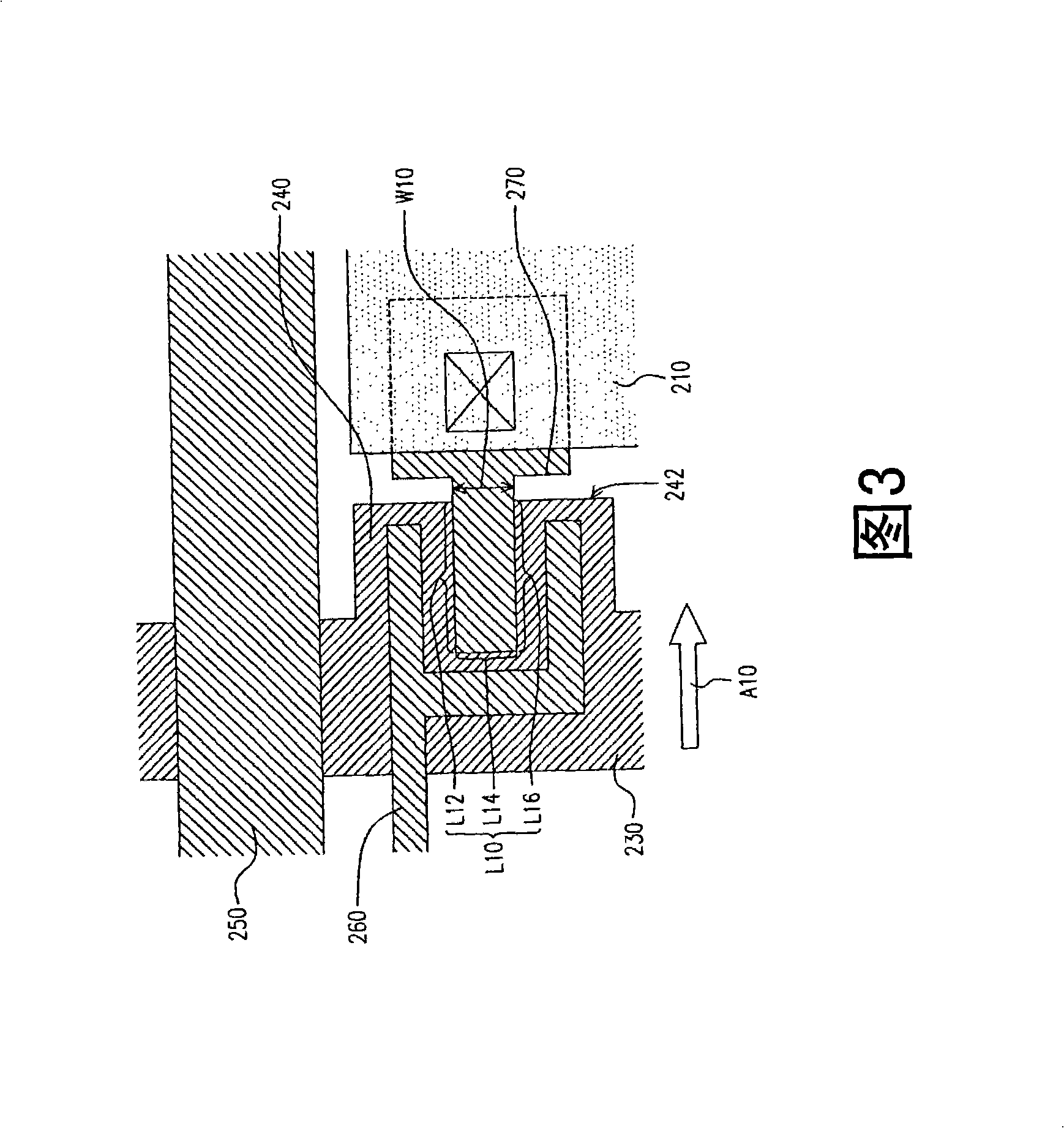
[0028] Referring to equation (1), ie V F =[C GD / (C LC +C ST +C GD )]×ΔV G , if [C GD / (C LC +C ST +C GD )] is set as a fixed constant k, then V can be obtained F =kΔV G . can be stored by the pixel storage capacitor C ST with gate / drain capacitance C GD The ratio of the error value is designed to conform to the above relationship, and the feedthrough voltage V of each pixel is F And the voltage difference ΔV of the scanning wiring when turning on (on) and turning off (off) the thin film transistor G maintain a constant proportional relationship. In more detail, the pixel storage capacitor C of each pixel ST with gate / drain capacitance C GD In any case, there is an error with the original design value due to the influence of process variation, and its V F with ΔV G The ratio between the two is constant and unaffected. Thus, at the drive voltage of V F In terms of compensation, more accurate compensation can be obtained, and the problem of screen flickering ...
PUM
 Abstract
Description
Claims
Application Information
 - R&D
- Intellectual Property
- Life Sciences
- Materials
- Tech Scout
- Unparalleled Data Quality
- Higher Quality Content
- 60% Fewer Hallucinations
Browse by: Latest US Patents, China's latest patents, Technical Efficacy Thesaurus, Application Domain, Technology Topic, Popular Technical Reports.
© 2025 PatSnap. All rights reserved.Legal|Privacy policy|Modern Slavery Act Transparency Statement|Sitemap|About US| Contact US: help@patsnap.com