Display device
A display device and node technology, applied to static indicators, instruments, electrical components, etc., can solve the problems of increasing the number of output pins of the driving LSI, increasing the cost of driving the LSI, and increasing the size of the edge, so as to reduce the number of pins The effect of reducing the number of control clock lines and reducing the edge size
- Summary
- Abstract
- Description
- Claims
- Application Information
AI Technical Summary
Problems solved by technology
Method used
Image
Examples
Embodiment 1
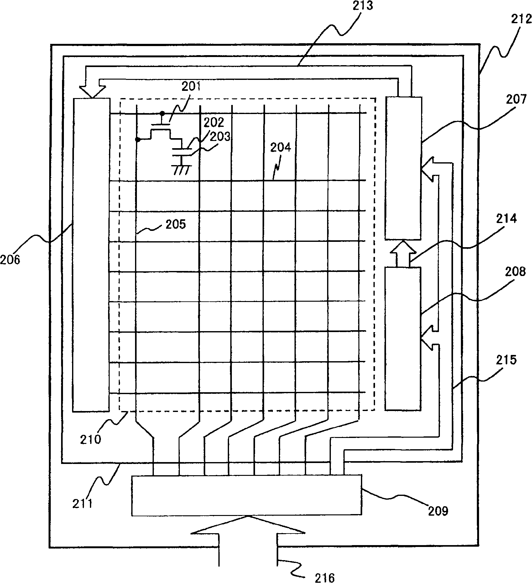
[0028] figure 1 A block diagram showing the configuration of the display device of this embodiment. exist figure 1 Among them, the display device of this embodiment is composed of a liquid crystal panel 211 on an insulating substrate 212 and a driving LSI (209) for driving it. In the liquid crystal panel 211, a plurality of gate lines 204 and drain lines 205 are respectively arranged in the horizontal direction and the vertical direction, and a pixel electrode 202, an opposing electrode 203, and a switching element 201 are arranged at intersections of the gate lines 204 and drain lines 205. The pixel portion forms the display area 210 . A power supply circuit 208 , a level shift circuit block 207 , and a gate driver circuit 206 are formed in a peripheral portion of the display region 210 , that is, an edge region.
[0029] The drive LSI (209) generates a control clock 215 to be supplied to the power supply circuit 208 and the level shift circuit block 207 based on the contr...
Embodiment 2
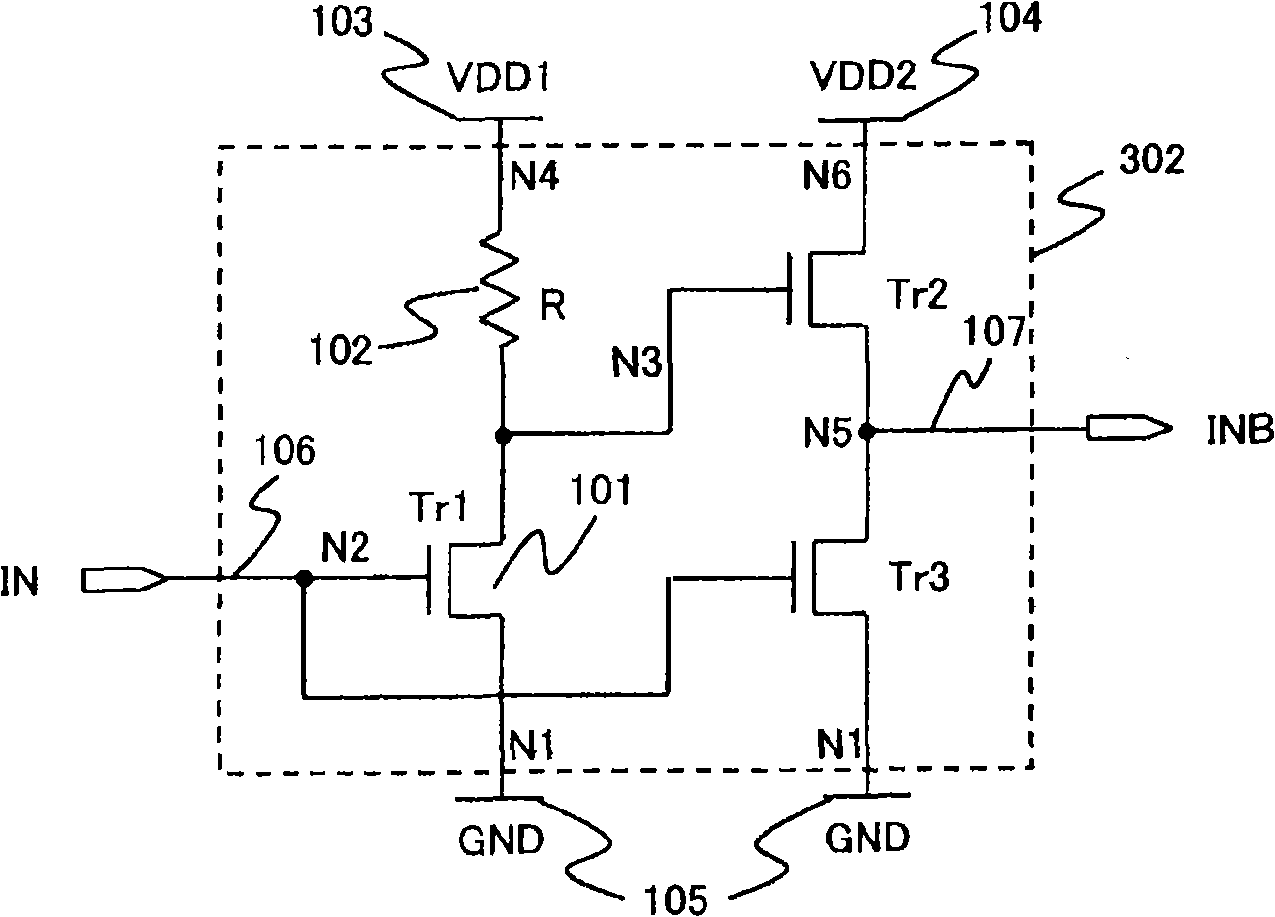
[0048] The inverter circuit of this embodiment reduces the influence of the CR time constant based on the resistive load R constituting the inverter circuit and the parasitic capacitance C of the transistor by setting a two-stage output buffer, and when the resistive load R is increased, the output is also realized. The rapid rise of the waveform. Below, use Figure 5 and Figure 6 , to illustrate this embodiment. It should be noted that the structure other than the inverter circuit is the same as that of the first embodiment, so the description thereof will be omitted.
[0049] Figure 5 is a structural diagram of the inverter circuit of this embodiment. exist Figure 5 Among them, the inverter circuit 302 includes an input inverter composed of a high-resistance load R and a transistor Tr1, an intermediate buffer composed of transistors Tr2 and Tr3, and an output buffer composed of transistors Tr4 and Tr5. The sources of the transistors Tr1 , Tr3 , and Tr5 are connected...
Embodiment 3
[0060] In this embodiment, by sharing the higher power supply voltage VDD1 used in the inverter circuit with the power supply voltage VDD of the level shift circuit block 207, the number of power supply voltages required for the operation of the built-in circuit is reduced, and the efficiency of the built-in circuit is reduced. Controls the reduction in the number of clock lines.
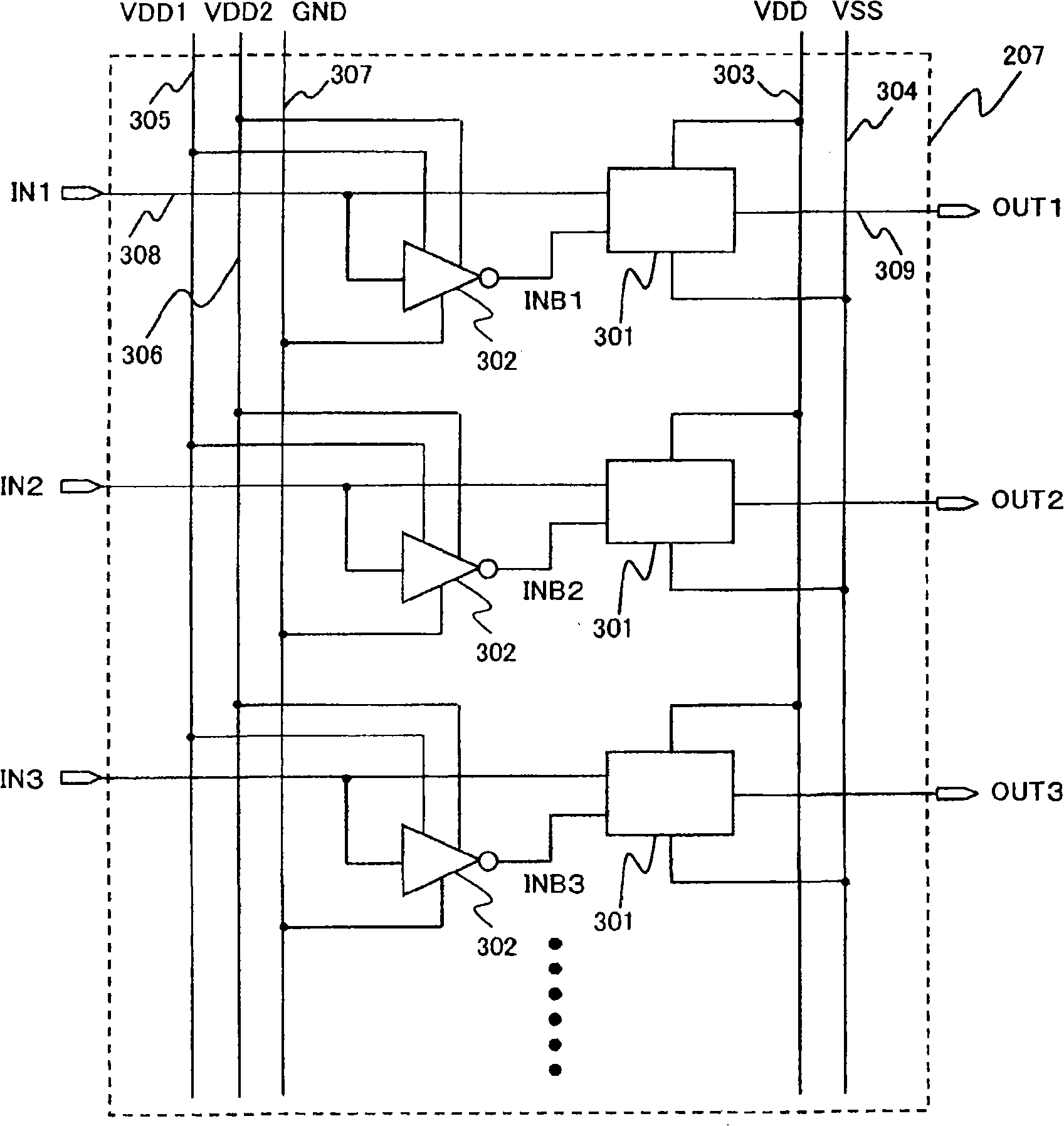
[0061] Figure 7 is a configuration diagram of the level shift circuit block 207 of this embodiment. exist Figure 7 , the level shift circuit block 207 is used to increase the figure 1 The level shift circuit 301 for controlling the amplitude of the control clock output by the drive LSI (209) and the inverter circuit 302 for generating the inverted clock INB required to operate the level shift circuit 301 are constituted. This inverter circuit 302 is the same as the inverter circuit 302 used in Embodiments 1 and 2, and its circuit configuration and operation were described in Embodiments 1 and 2...
PUM
 Abstract
Description
Claims
Application Information


