Semiconductor device

A semiconductor and conductive terminal technology, applied in the direction of semiconductor devices, semiconductor/solid-state device components, electric solid-state devices, etc., can solve the problems of approaching the limit, difficult to realize the miniaturization of semiconductor devices, electromagnetic interference, and low impedance at the same time. Achieving the effect of miniaturization

Inactive Publication Date: 2008-10-22
SANYO ELECTRIC CO LTD +1
View PDF2 Cites 3 Cited by
  • Summary
  • Abstract
  • Description
  • Claims
  • Application Information

AI Technical Summary

Problems solved by technology

However, since these wirings are sometimes wound long in the layout design, if the semiconductor chip and the capacitor element are separate components, there is a limit to the proximity of the two.
[0011] As described above, in the structure provided with an external capacitive element, it is difficult to achieve both the miniaturization of the semiconductor device and the further reduction of the influence of electromagnetic interference.
[0012] On the other hand, as described in the above-mentioned patent document 2, in the conventional structure in which the capacitive element is formed in the same semiconductor device, compared with the case of using an external capacitive element, it is possible to achieve low impedance and low inductance of the wiring. However, in order to obtain sufficient electrostatic capacitance to effectively remove high-frequency electromagnetic interference, a large area is required
[0013] Therefore, there is a problem that the miniaturization of the semiconductor device cannot be achieved due to the formation of functional elements other than the capacitive element (for example, a drive circuit composed of transistors, logic circuits, or wiring connected to them) on the same semiconductor substrate.

Method used


Image

  • Semiconductor device
  • Semiconductor device
  • Semiconductor device

Examples


Embodiment Construction

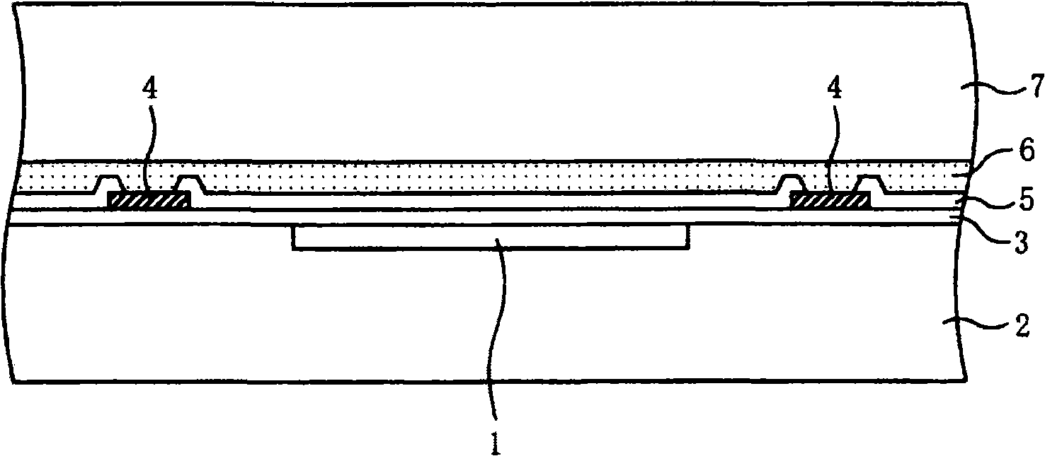
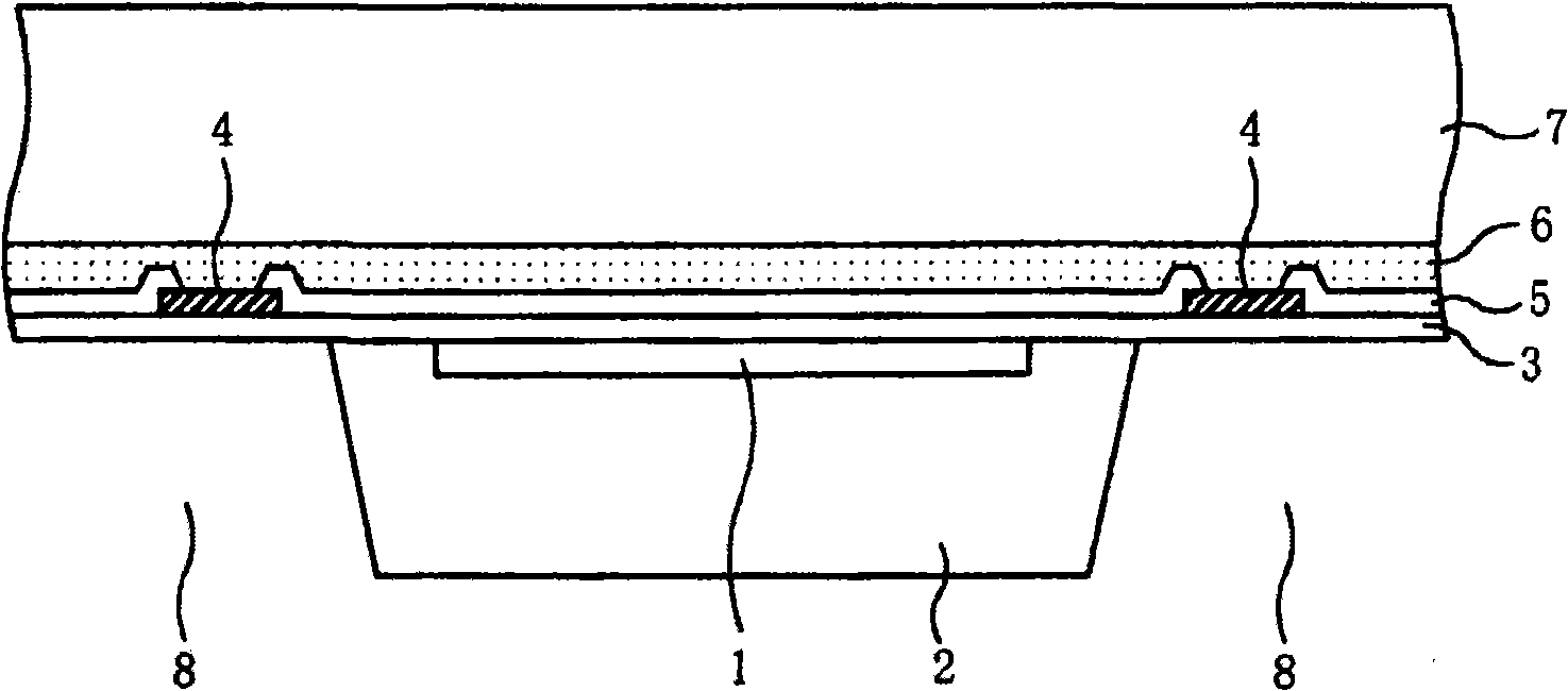
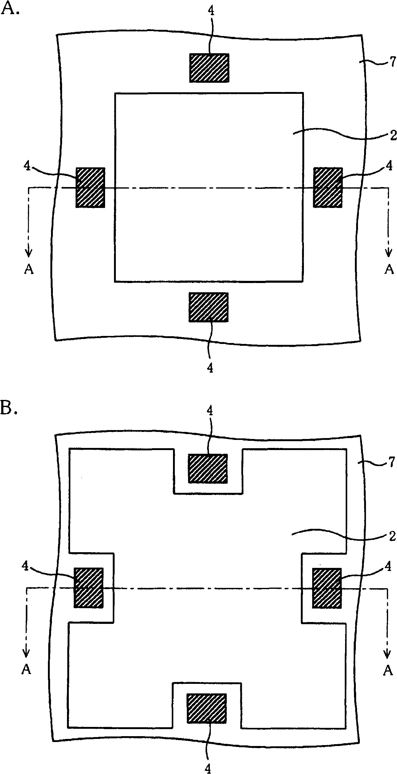
[0046] Next, a first embodiment of the present invention will be described with reference to the drawings. Figure 1 to Figure 9 A sectional view or a plan view showing the sequence of the manufacturing process, respectively. In addition, the manufacturing process described below is performed using a wafer-shaped semiconductor substrate, and a plurality of semiconductor devices are formed in an array with predetermined scribe lines as boundaries. For convenience, a process of forming one of the semiconductor devices will be described.

[0047] First, if figure 1 As shown, a semiconductor substrate 2 made of silicon (Si) or the like is prepared, and a semiconductor integrated circuit 1 (such as photosensitive elements such as CCD sensors, CMOS sensors, and illuminance sensors, light-emitting elements, and semiconductors such as transistors) is formed on the surface of the semiconductor substrate 2. A drive circuit, a logic circuit, or wiring connected to them, which are formed...


PUM


Abstract

The purpose of the invention is to provide a semiconductor device, having a capacitance component in a same semiconductor device to minimize the whole device, and having a capacitance component having large static capacitance compared with a current semiconductor device. The semiconductor device has a semiconductor circuit (1) and a pad electrode (4) on a surface of the semiconductor substrate (2). A second insulating film (10) is formed on a side face and a back of the semiconductor substrate (2). A capacitance electrode (9) is formed between the back of the semiconductor substrate (2) and the second insulating film (10), in contact with the back of the semiconductor substrate (2). The second insulating film (10) is covered by a wiring layer (11) connected to the pad electrode (4) electrically. The wiring layer (11) and the capacitance electrode (9) are overlapped through the second insulating film. Therefore, the capacitance (16) is formed of the capacitance electrode (9), the second insulating film (10) and the wiring layer (11).

Description

technical field [0001] The present invention relates to a semiconductor device including a capacitive element. Background technique [0002] From the viewpoint of reducing the influence of voltage level fluctuations caused by electromagnetic interference and preventing malfunctions of semiconductor chips, conventionally, capacitors called bypass capacitors are provided on the terminals (power supply terminals, ground terminals) of the semiconductor chips. element. [0003] For example, Patent Document 1 below discloses a semiconductor device in which a semiconductor chip and an external capacitive element called a chip capacitor are mounted on the same substrate and packaged as a whole as a chip. [0004] In addition, the following Patent Document 2 discloses a semiconductor device in which a capacitive element functioning as a bypass capacitor is formed using multilayer wiring layers on a semiconductor substrate and an interlayer insulating film therebetween. [0005] Tec...

Claims


Application Information

Patent Timeline
Patent Type & Authority Applications(China)
IPC IPC(8): H01L27/06H01L23/485H01L23/552
CPCH01L2924/30107H01L2924/01074H01L2924/01006H01L2224/1132H01L24/12H01L23/3114H01L23/481H01L2924/30105H01L2924/00013H01L24/32H01L27/14683H01L24/11H01L2224/05644H01L2224/0558H01L2924/04941H01L2924/01073H01L23/642H01L27/14618H01L2924/01022H01L2924/01005H01L2924/01033H01L24/25H01L2924/01047H01L2924/01079H01L2924/01013H01L23/5223H01L2924/14H01L2924/014H01L2924/01078H01L24/29H01L2924/19043H01L2924/3011H01L2924/19041H01L2224/02313H01L2924/01029H01L2924/09701H01L2224/131H01L2924/04953H01L2224/18H01L2224/0401H01L2924/3511H01L2924/3512H01L2224/13099H01L2924/00
Inventor 堀越胜内山久嘉野间崇关嘉则山田紘士石部真三篠木裕之
Owner SANYO ELECTRIC CO LTD
Why Eureka
Try Eureka