

Highly efficient stacked thin-film solar cell of nano silicon
A nano-silicon thin film and solar cell technology, applied in the field of solar cells, can solve the problems of high production costs, limiting the development prospects of amorphous silicon thin film solar cells, and expensive substrates
Inactive Publication Date: 2008-10-22
无锡市纳微电子有限公司
View PDF0 Cites 3 Cited by
- Summary
- Abstract
- Description
- Claims
- Application Information
AI Technical Summary
Problems solved by technology
At present, in the manufacture of solar cells, products based on crystalline silicon and polycrystalline silicon are the leading products, and their market share is about 80%. Silicon materials are currently the main raw materials for solar cells. In the cost share of cells, Silicon material accounts for nearly 40%. Due to the high price of its base material and high production cost, it affects the development of solar cells.
The amorphous silicon thin-film solar cells developed in recent years use glass, steel plates and organic thin films as substrates. The film thickness of amorphous silicon is 1 μm, which is less than 1 / 100 of the thickness of crystalline silicon cells, which greatly reduces the manufacturing cost. , and can be made into larger area products, but its photothermal stability (S-W effect) of amorphous silicon solar cells is poor, and its conversion efficiency η value is much lower than that of crystalline silicon solar cells, and the stability of its products And reliability is also poor, thus limiting the development prospects of amorphous silicon thin film solar cells
Method used
View moreImage
Smart ImageViewing Examples

Examples
Embodiment Construction
Login to View More PUM
 Abstract
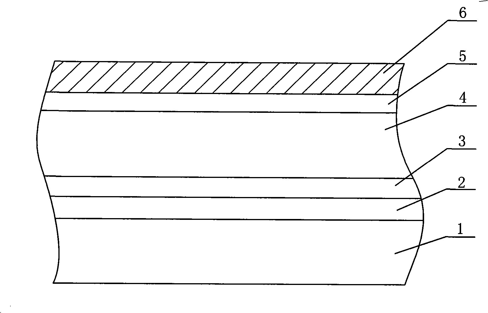
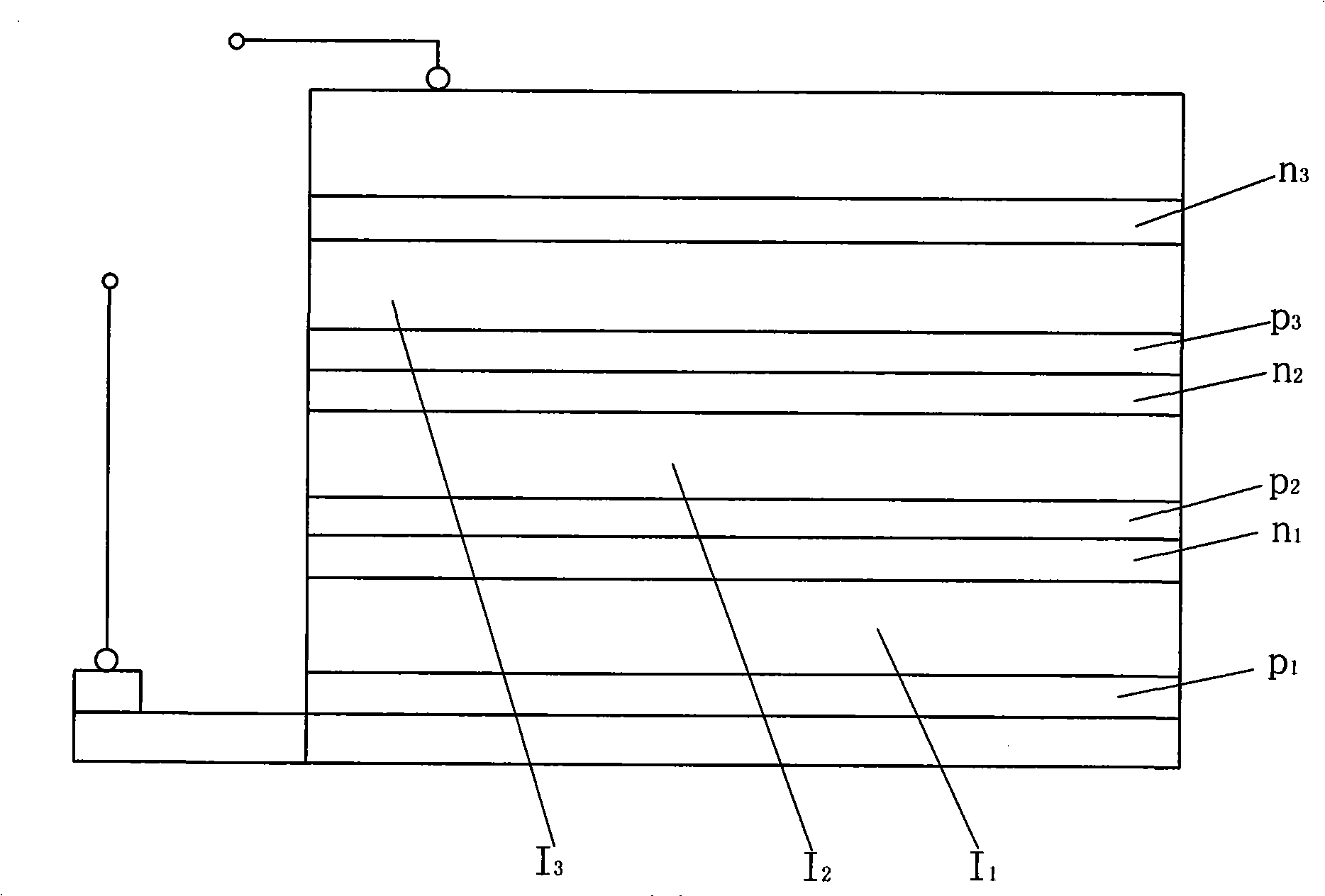
The invention relates to a stacked high-efficient nano silicon film solar cell. The stacked high-efficient nano silicon film solar cell has good photo-thermal stability, high conversion efficiency, good stability and reliability and low production cost, and comprises a cell substrate (1) the materials of which are glass or organic films, wherein, a PIN structures are arranged on the substrate (1); each PIN structure comprises a conductive film (2); a layer of boron P type amorphous silicon film (3) is grown on the conductive film (2); the crystalline state ratio Xc of the film is changed to form a variable bandgap nano silicon buffer layer (4); a layer of N type nano silicon film (5) is grown on the variable bandgap nano silicon buffer layer (4) by filling of phosphorane (PN3); and an electrode Ag / Al is coated on the silicon film (5). The stacked high-efficient nano silicon film solar cell is characterized in that: the crystalline state ratio xc of the variable bandgap nano silicon buffer layer (4) is between 40 and 53; the PIN structures are stacked; the conductive film (2) of a PIN structure which is positioned on the bottom layer covers the substrate (1); and the electrode Ag / Al covers the silicon film (5) of a PIN structure which is positioned on the top layer.
Description
A stacked high-efficiency nano-silicon thin-film solar cell (1) Technical field The invention relates to the technical field of solar cells, in particular to a laminated high-efficiency nano-silicon thin-film solar cell. (2) Background technology At present, in the manufacture of solar cells, products based on crystalline silicon and polycrystalline silicon are the leading products, and their market share is about 80%. Silicon materials are currently the main raw materials for solar cells. In the cost share of cells, Silicon material accounts for nearly 40%, because of its expensive base material and high production cost, which affects the development of solar cells. The amorphous silicon thin-film solar cells developed in recent years use glass, steel plates and organic thin films as substrates. The film thickness of amorphous silicon is 1 μm, which is less than 1 / 100 of the thickness of crystalline silicon cells, which greatly reduces the manufacturing cost. , and can ...
Claims
Login to View More Application Information
Patent Timeline
 IPC IPC(8): H01L31/075H01L31/036H01L31/076
CPCY02E10/50Y02E10/548
Inventor王树娟何宇亮
Owner无锡市纳微电子有限公司