LCD device and image element array substrates

A technology for pixel array substrates and liquid crystal display devices, applied in optics, instruments, electrical components, etc., can solve problems affecting display quality, flicker, etc., achieve optimized image quality performance, reduce flicker, and reduce capacitive coupling problems Effect

Active Publication Date: 2008-10-29
KUSN INFOVISION OPTOELECTRONICS
View PDF1 Cites 14 Cited by
  • Summary
  • Abstract
  • Description
  • Claims
  • Application Information

AI Technical Summary

Problems solved by technology

[0013] Figure 4 for image 3 The schematic diagram of the polarity of each sub-pixel in the pixel array structure, as shown in the figure, although the polarities of the two sub-pixel electrodes in the same pixel are opposite, the polarity of the adjacent sub-pixels between two adjacent pixels is the same, so that The problem of capacitive coupling will also cause flicker (Flicker) when displaying, which will affect the display quality

Method used


Image

  • LCD device and image element array substrates
  • LCD device and image element array substrates
  • LCD device and image element array substrates

Examples


Embodiment Construction

[0026] In order to make the object, technical solution and advantages of the present invention clearer, the specific implementation manners of the present invention will be described below in conjunction with the accompanying drawings.

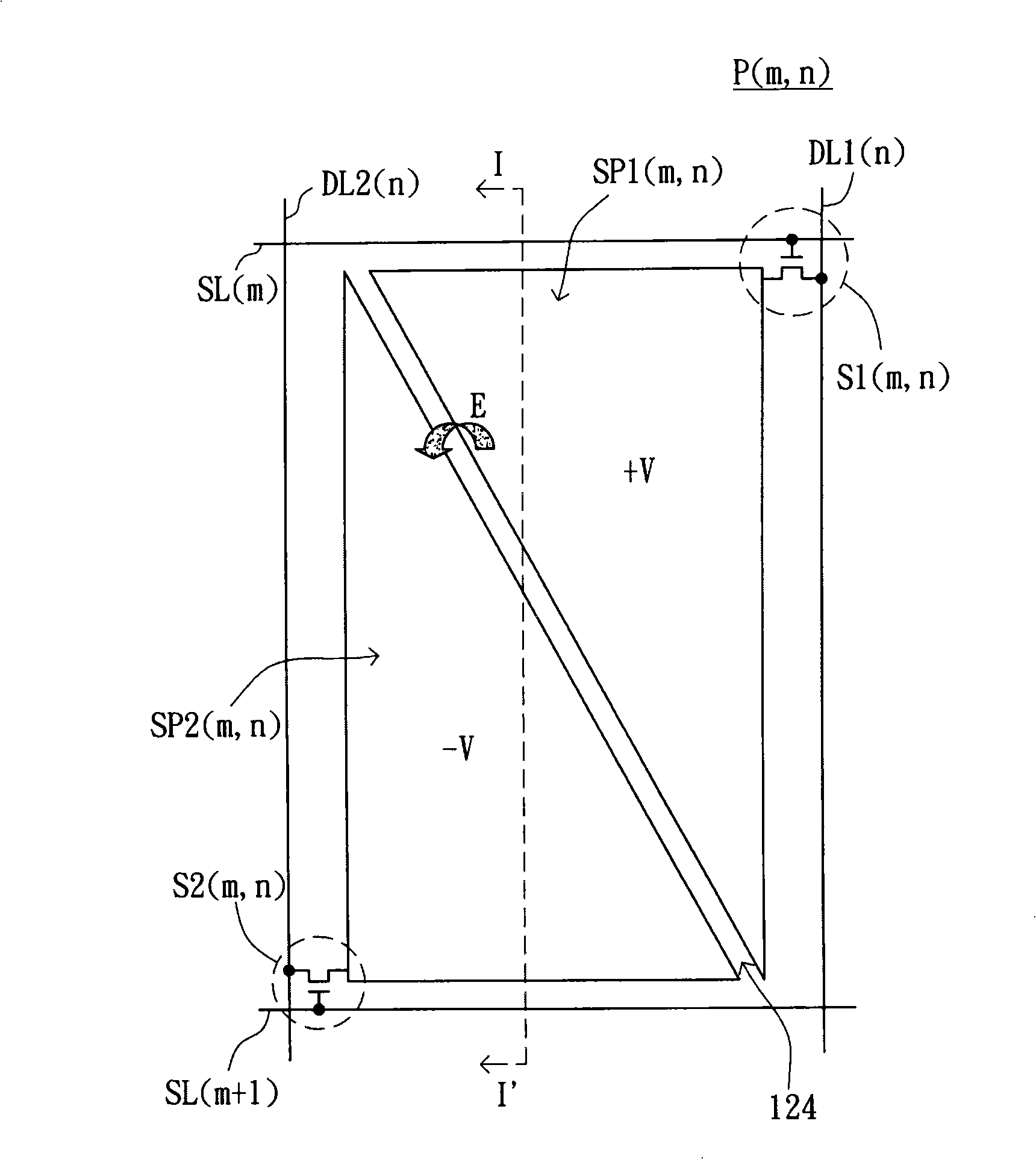
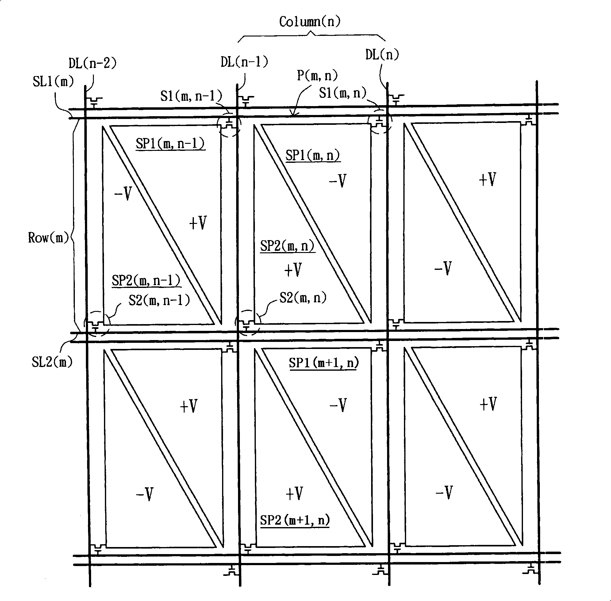
[0027] Such as Figure 5 Shown is a schematic diagram of the pixel array structure of the present invention. Here, the data line on the left side of the pixel electrode is used to define the vertical coordinate of the pixel electrode, and the pair of scanning lines corresponding to the pixel electrode is used to define the horizontal coordinate of the pixel electrode. The yth data line DL(y) and the xth pair of scan lines SL1(x) and SL2(x) corresponding to the pixel electrodes are defined. Similarly, the pixel electrode P(x+1, y+1) is the (x+1)th data line DL(y+1) on the left side of the pixel electrode corresponding to the (x+1)th data line DL(y+1). Defined for scan lines SL1(x+1) and SL2(x+1).

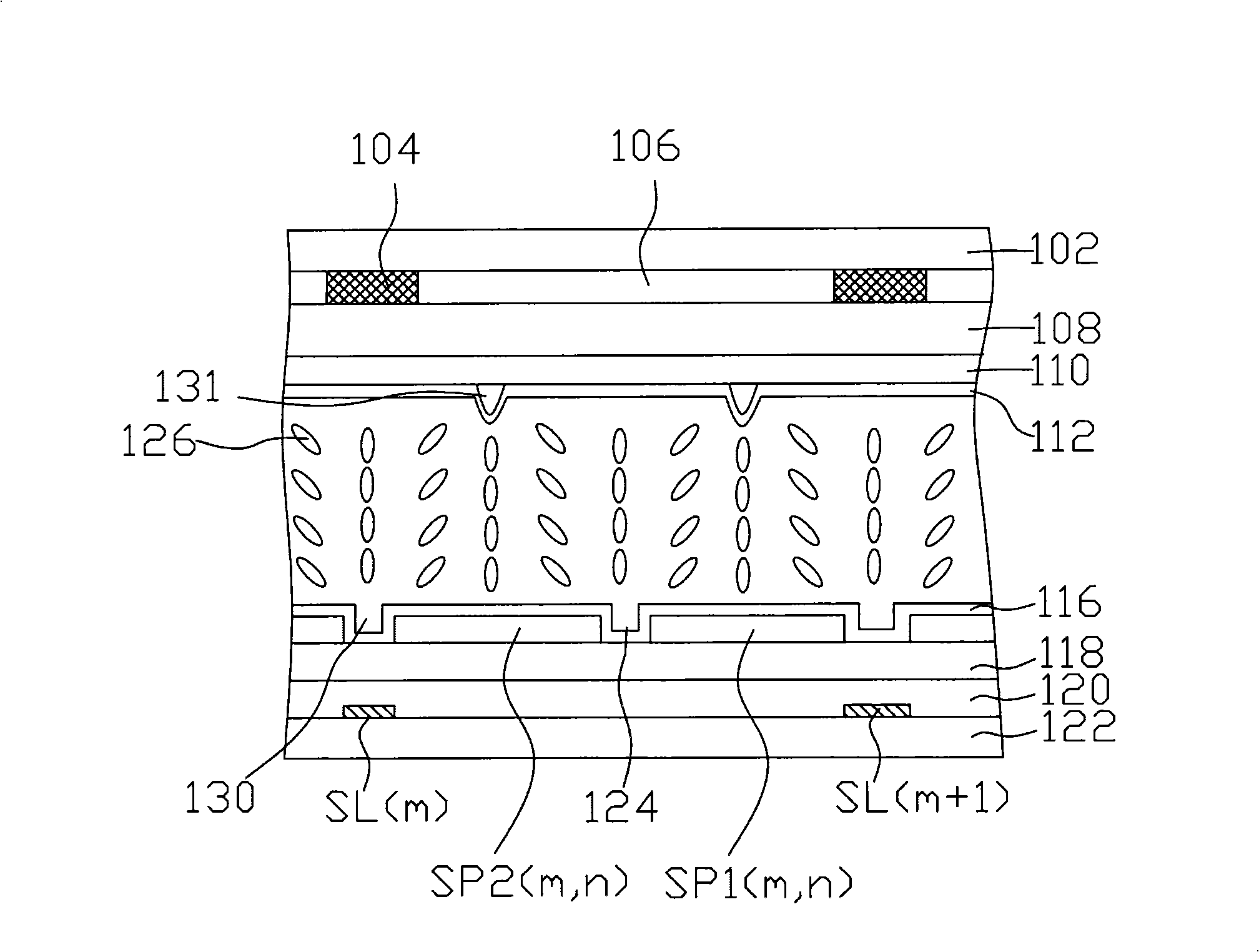
[0028] Such as Image 6 shown, for Figur...


PUM


Abstract

The invention provides a liquid crystal display device and a pixel array substrate thereof, wherein, the pixel array substrate includes: a plurality of pixel electrodes formed on the substrate, and each pixel electrode is provided with two sub-pixel electrodes; a plurality of switching elements formed on the substrate, and each switching element is electrically connected with one sub-pixel electrode; a plurality of data lines formed on the substrate, electrically connected with the switching elements corresponding to a plurality of sub-pixels, and used for exerting voltage signals with opposite polarities to two neighboring sub-pixel electrodes. The liquid crystal display device and the pixel array substrate thereof are used for solving the control problem of the sub-pixels and improving the expressive capability of picture quality.

Description

technical field [0001] The present invention relates to the technical field of liquid crystal display, and in particular relates to a liquid crystal display device with high display quality and a pixel array substrate thereof. Background technique [0002] Liquid crystal display devices have the advantages of lightness, thinness, and low power consumption, and are widely used in modern information equipment such as computers, mobile phones, and personal digital assistants. Currently, the performance requirements of the market for liquid crystal display devices are: high contrast, high brightness, high color saturation, fast response, and wide viewing angle. [0003] In order to achieve a wide viewing angle, a variety of technologies have been developed in the prior art, such as: twisted nematic liquid crystal display (TN) plus wide viewing film (wide viewing film), in-plane switching (In-plane switching, IPS) Liquid crystal display devices, fringe field switching (Fringe Fi...

Claims


Application Information

Patent Timeline
Patent Type & Authority Applications(China)
IPC IPC(8): G02F1/1362H01L27/12
Inventor 钟德镇邱郁雯廖家德简廷宪
Owner KUSN INFOVISION OPTOELECTRONICS
Why Eureka
Try Eureka