

MOSFET device with silicon carbide single-side deep L-shaped base region structure and preparation method of MOSFET device
A silicon carbide single and base technology, applied in the field of microelectronics, can solve the problems affecting the forward blocking characteristics of the device, and achieve the effect of reducing the Miller platform, reducing the heat dissipation requirements, and reducing the electric field concentration
- Summary
- Abstract
- Description
- Claims
- Application Information
AI Technical Summary
Problems solved by technology
Method used
Image

Examples
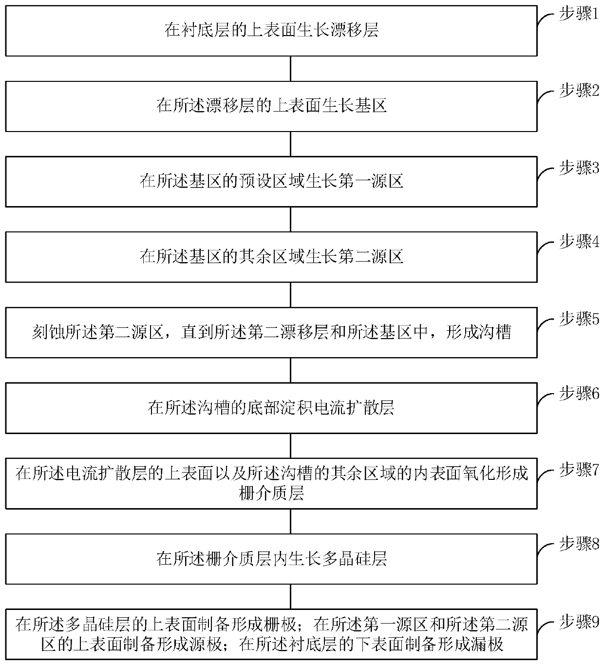
Embodiment 1
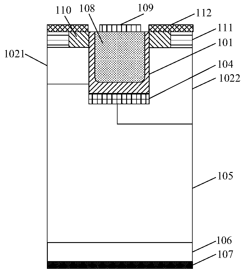
[0049] See figure 1 , figure 1 A schematic cross-sectional structure diagram of a MOSFET device with a silicon carbide single-side deep L-shaped base structure provided by an embodiment of the present invention.
[0050] A MOSFET device with a silicon carbide single-side deep L-shaped base structure, comprising:
[0051] gate dielectric layer 101;
[0052] The base region 102, the base region 102 includes a first base region 1021 and a second base region 1022, which are respectively located on both sides of the gate dielectric layer 101, wherein the second base region 1022 is a P-type base region with a deep L-shaped structure in section;
[0053] The current diffusion layer 104 is located between the gate dielectric layer 101 and the second base region 1022;
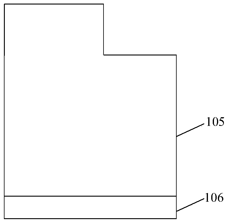
[0054] The drift layer 105 is located on the lower surface of the base region and the current diffusion layer 104;
[0055] The substrate layer 106 is located on the lower surface of the drift layer 105;
[0056] T...
PUM
 Abstract
Description
Claims
Application Information