Inductance coil and inductance coupling plasma processing device

A plasma and processing device technology, applied in the field of ion processing equipment, can solve the problems of crystal element influence, waste of radio frequency energy, unreliable ignition of plasma, etc.

Active Publication Date: 2015-05-20
ADVANCED MICRO FAB EQUIP INC CHINA
View PDF8 Cites 5 Cited by
  • Summary
  • Abstract
  • Description
  • Claims
  • Application Information

AI Technical Summary

Problems solved by technology

[0004] However, such a reaction chamber structure will also bring serious problems: due to the existence of the Faraday shield, the electric field generated on the induction coil cannot enter the reaction chamber, and only part of the magnetic field can enter, which will cause the plasma to be unable to be reliably ignited when the plasma is ignited. , additional devices or higher power input RF coils are required to ensure plasma ignition
The impedance of the plasma will change sharply before and after ignition, from a high-impedance substance to a conductor in an instant, and the matching device that adjusts the input RF power needs a mechanical structure to adjust the impedance matching, which can only reach the second level, so the response speed of the matching device It is far from the impedance change at the moment of ignition, so the extra power applied to ignite the plasma will be wrongly applied to the reaction chamber for a period of time, during which the excessive power will damage the components in the reaction chamber or the parts to be processed. of wafers adversely affect the
At the same time, due to the existence of the Faraday shielding plate, only part of the radio frequency magnetic field can enter the reaction chamber to excite the reaction gas to form plasma, and part of the radio frequency energy is wasted, which greatly reduces the use efficiency of electric energy

Method used


Image

  • Inductance coil and inductance coupling plasma processing device
  • Inductance coil and inductance coupling plasma processing device
  • Inductance coil and inductance coupling plasma processing device

Examples


Embodiment 1

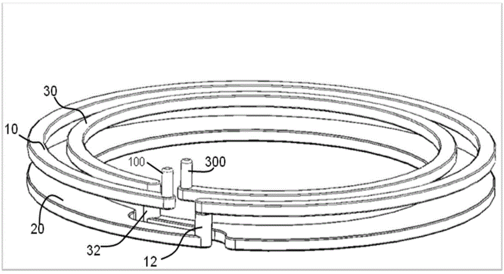
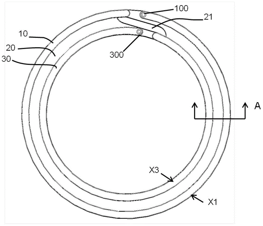
[0023] See figure 1 , which is a schematic diagram of the structure of the inductance coil of the present invention. The inductance coil of the present invention includes a first coil 10 and is connected to a radio frequency power supply or other external circuits through a radio frequency input connection part 100 . The inductance coil of the present invention also includes an intermediate coil 20 located below the first coil, the intermediate coil is in the shape of a flat plate, and its width is larger than that of the first coil 10 . The first coil 10 forms a circular ring, one end is a connecting portion 100 , and the other end is connected to the intermediate coil 20 through a downward first intermediate connecting portion 12 . The middle coil forms a ring, one end is the first connecting part 12 , and the other end is the second middle connecting part 32 . The second intermediate connecting portion extends upward from the surface of the intermediate coil 20 and is con...


PUM


Abstract

The invention discloses a plasma processing device which comprises an airtight reaction cavity. The reaction cavity comprises reaction cavity side walls and an insulating material window at the top, a base used for supporting a to-be-processed substrate is arranged in the reaction cavity, and a self-shielding inductance coil is fixed above the insulating material window. The plasma processing device is characterized in that the self-shielding inductance coil comprises a first coil, a middle coil and a third coil which are serially connected with one another, the middle coil is positioned below the first coil and the third coil, width of the middle coil is larger than that of the first coil or the third coil, a radio frequency power source applies a radio frequency electric field to space between an input end of the first coil and an output end of the third coil of the self-shielding inductance coil, the output end of the third coil is further connected with a balance adjusting circuit to enable standing waves on the self-shielding inductance coil, and voltage amplitude of the middle coil is smaller than that on the first coil or the third coil.

Description

technical field [0001] The invention relates to plasma processing equipment, in particular to an inductive coupling coil of a plasma processing device. Background technique [0002] In recent years, with the development of semiconductor manufacturing processes, the requirements for the integration and performance of components are getting higher and higher, and plasma technology (Plasma Technology) has been widely used. Plasma technology introduces a reactive gas and electron flow into the reaction chamber of the plasma processing device, uses a radio frequency electric field to accelerate the electrons, and collides with the reactive gas to ionize the reactive gas and generate plasma. The generated plasma can be used Used in various semiconductor manufacturing processes, such as deposition processes (such as chemical vapor deposition), etching processes (such as dry etching), etc. [0003] Plasma processing equipment includes common capacitively coupled and inductively cou...

Claims


Application Information

Patent Timeline
Patent Type & Authority Applications(China)
IPC IPC(8): H01J37/32H01F38/14
CPCH01F38/14H01J37/32798
Inventor 倪图强梁洁
Owner ADVANCED MICRO FAB EQUIP INC CHINA
Why Eureka
Try Eureka