Solid-state imaging device, signal processing method for the same, and imaging apparatus
一种固态成像、信号处理的技术,应用在图像通信、辐射控制装置、电视等方向,能够解决降低电源电压、降低等问题,达到防止固定模式噪声和随机噪声、提高图像质量的效果
Inactive Publication Date: 2008-10-29
SONY CORP
View PDF2 Cites 10 Cited by
- Summary
- Abstract
- Description
- Claims
- Application Information
AI Technical Summary
Problems solved by technology
(1) Since the maximum amount Qfd.max of the accumulated charge must be larger than the maximum amount Qpd.max of the accumulated charge in the photoelectric conversion element, there is a limit to lowering the capacitance of the floating diffusion transistor 106 in order to improve the charge-voltage conversion efficiency
(2) For the same reason as above, a decrease in the power supply voltage Vdd serving as a reset voltage of the floating diffusion capacitor 106 causes a decrease in the maximum amount Qfd.
Method used
View moreImage
Smart ImageViewing Examples


Examples
no. 1 example
no. 2 example
no. 3 example
Login to View More PUM
 Abstract
Disclosed herein is a solid-state imaging device, including, a pixel array unit, driving means, signal processing means, level determining means and control means.
Description
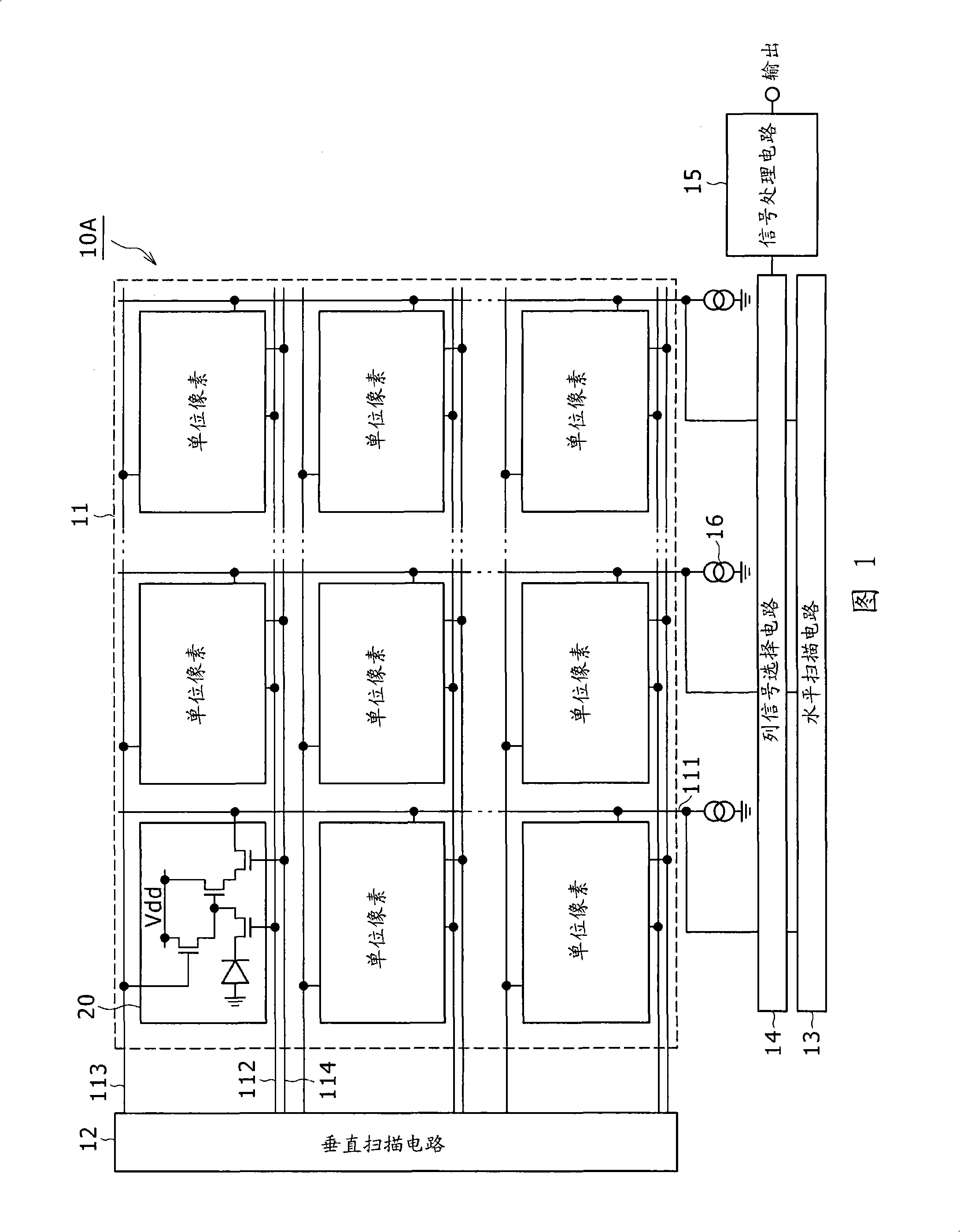
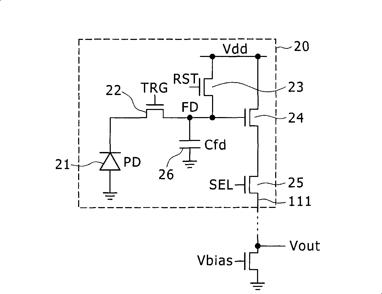
Solid-state imaging device, signal processing method thereof, and imaging device technical field The present application relates to a solid-state imaging device, a signal processing method thereof, and an imaging device. Background technique FIG. 36 shows a configuration example of the unit pixel 100 of the solid-state imaging device 100 . As in this example, in the unit pixel 100 having the transfer transistor for transferring the signal charge obtained by the photoelectric conversion in the photoelectric conversion element 101, the accumulation of the floating diffusion capacitor (FD) that can be transferred to the unit pixel The maximum amount Qfd.max of charges is much larger than the maximum amount Qpd.max of accumulated charges in the photoelectric conversion element 101 as a light receiving unit. As a result, perfect transfer of signal charges from the photoelectric conversion element 101 to the floating diffusion capacitor 106 is achieved by removing the remaining...
Claims
Login to View More Application Information
Patent Timeline
 Patent Type & Authority Applications(China)
IPC IPC(8): H04N3/15H04N5/335H04N23/40H01L27/146H04N25/00H04N25/46
CPCH04N5/37457H04N5/357H04N5/378H04N25/583H04N25/778H04N25/78H04N25/618H04N25/677H04N25/76H04N25/60H04N25/75
Inventor 大池佑辅
Owner SONY CORP
Features
- R&D
- Intellectual Property
- Life Sciences
- Materials
- Tech Scout
- Unparalleled Data Quality
- Higher Quality Content
- 60% Fewer Hallucinations
Learn More Browse by: Latest US Patents, China's latest patents, Technical Efficacy Thesaurus, Application Domain, Technology Topic, Popular Technical Reports.
© 2025 PatSnap. All rights reserved.Legal|Privacy policy|Modern Slavery Act Transparency Statement|Sitemap|About US| Contact US: help@patsnap.com